
Novel UMOS-like gate-controlled thyristor structure for ESD protection

a thyristor structure and gate control technology, applied in the direction of thyristor, electric devices, transistors, etc., can solve the problems of not being functional in lvtscr's with shallow trench isolation (sti), especially on epi, and achieve the effect of adding any process complexity and cos

Inactive Publication Date: 2002-09-19
CHARTERED SEMICONDUCTOR MANUFACTURING
View PDF0 Cites 17 Cited by
  • Summary
  • Abstract
  • Description
  • Claims
  • Application Information

AI Technical Summary

Benefits of technology

[0008] It is an object of the present invention is to provide a MOS gate-controlled SCR (UGSCR) structure for an ESD protection circuit in an IC device that is compatible with shallow trench isolation (STI) and self-aligned silicide (salicide) fabrication technology without adding any process complexity and cost.
[0010] It is yet another object of the present invention to provide the UGSCR with a low impedance state when "on", of about 1 to 3 ohms to make the UGSCR a low power dissipating device for ESD protection.

Problems solved by technology

Recently, reports have shown that LVTSCR's with shallow trench isolation (STI), especially on epi, are not functional because the hole current cannot efficiently forward bias the n+ cathode / p-substrate junction.

Method used


Image

  • Novel UMOS-like gate-controlled thyristor structure for ESD protection
  • Novel UMOS-like gate-controlled thyristor structure for ESD protection
  • Novel UMOS-like gate-controlled thyristor structure for ESD protection

Examples


Embodiment Construction

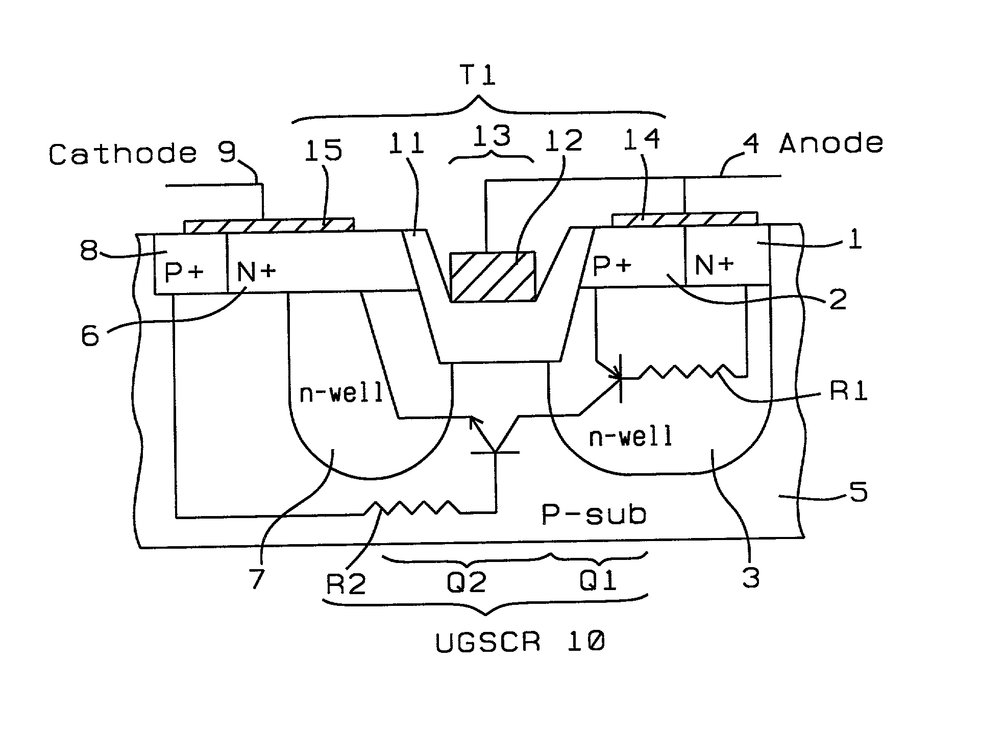
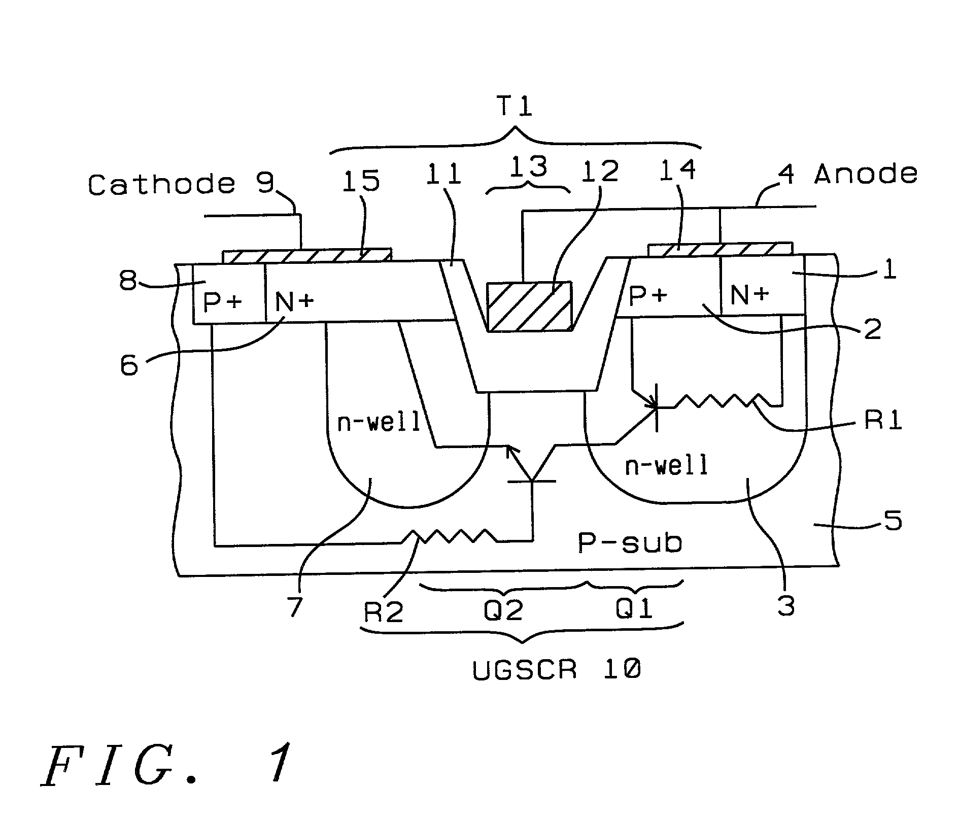
[0018] In the invention, a novel U-gate MOS (UMOS)-like gate-controlled SCR structure (UGSCR) is provided, see FIG. 1. The adjacent n+ (1) and p+ (2) diffusions in the n-well (3) are connected to the input terminal (4). A vertical parasitic pnp device (transistor) is formed with the p-substrate (5) as the collector, n-well (3) as the base, and input p+ (2) diffusion as the emitter. The n+ (6) diffusion partially on the n-well (7) located in the p-substrate (5), along with a p+ pick-up (8), is connected to the ground (9) or substrate bus and forms the emitter of the parasitic npn transistor. The base of the parasitic npn transistor is formed by the p-substrate (5) and the collector is the n-well (3) and the n-well contact (1). A UMOS-like MOS gate structure (13), comprised of a layer of silicon dioxide (11) and polysilicon gate (12) is formed between the two n-wells (3 and 7) and its gate (12) is connected to the input terminal (4).

[0019] The UGSCR structure is compatible with the se...


PUM


Abstract

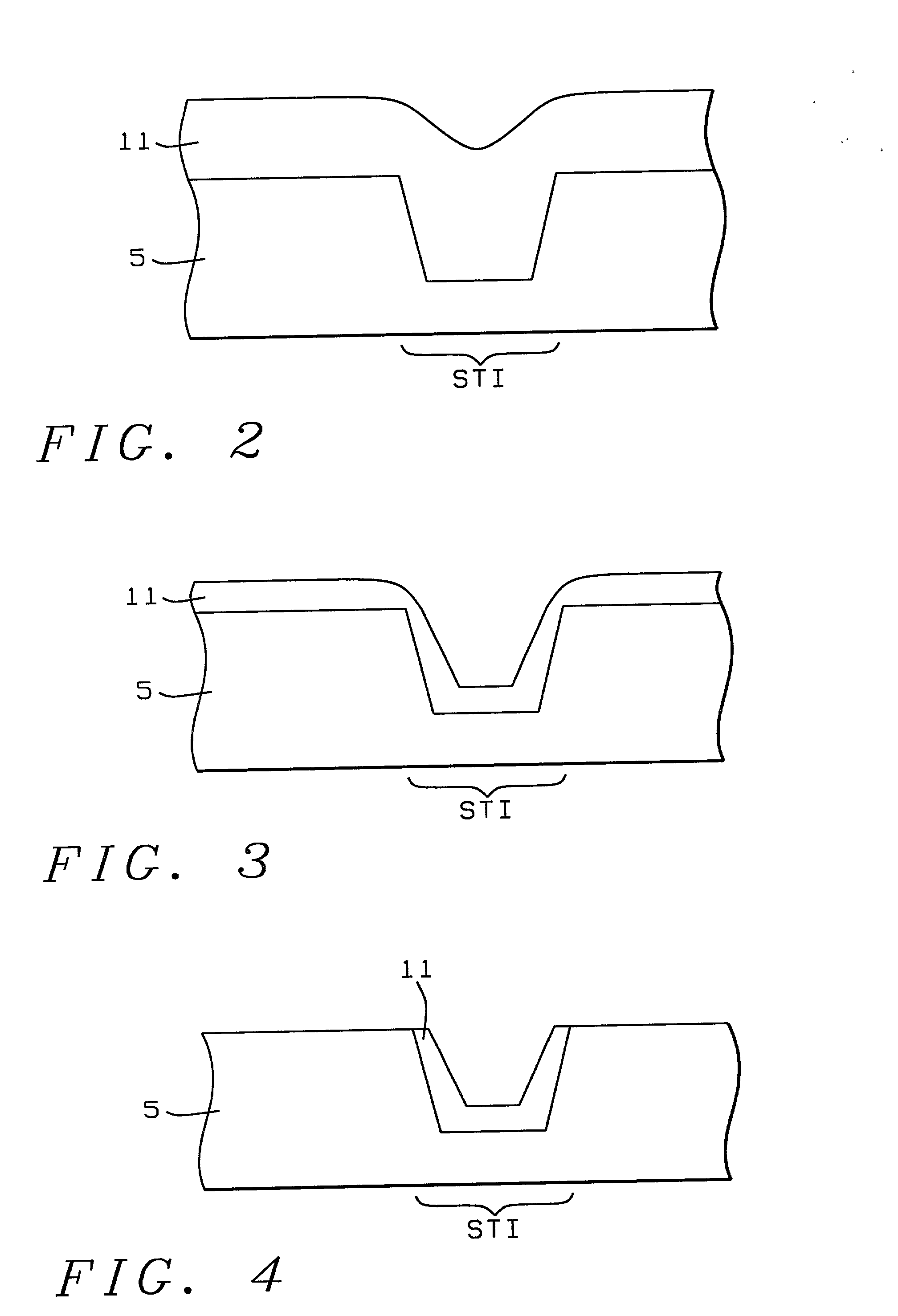
Described is a MOS gate-controlled SCR (UGSCR) structure with a U-shaped gate (UMOS) for an ESD protection circuit in an IC device which is compatible with shallow trench isolation (STI) and self-aligned suicide (salicide) fabrication technology. The UMOS gate is located in a p-substrate and is surrounded by an n-well on either side. Adjacent to one side of the UMOS gate, a first n+ diffusion is formed which straddles the first n-well. The n+ diffusion together with a p+ pickup diffused next to it form the cathode of the SCR (thyristor). Adjacent to the other side of the UMOS gate, a second n+ and p+ diffusion are formed in a second n-well. The second n+ and p+ diffusion together with the UMOS gate form the anode of the SCR and the input terminal of the circuit to be protected. The SCR is formed by the first n+ diffusion / n-well (cathode), the p-substrate, the second n-well and the second p+ / n+diffusion (anode). A latchup immune circuit is achieved by creating a U-shaped gate structure which is lined with a thick gate oxide--similar to a field oxide--under the poly gate.

Description

BACKGROUND OF THE INVENTION[0001] 1. Field of the Invention[0002] The invention relates to electrostatic discharge (ESD) structures for sub-micron devices, and more particularly to a thyristor (silicon controlled rectifier) which is gated by a U-type gate structure of a MOS (UMOS) transistor.[0003] 2. Description of the Related Art[0004] The Silicon Controlled Rectifier (SCR) is the most efficient of all protection devices in terms of ESD performance per unit area. Usually, the SCR trigger level is quite high. The Low Voltage Trigger SCR (LVTSCR) is the most promising device for ESD protection by surface channel to reduce the drain-tap junction avalanche breakdown. Recently, reports have shown that LVTSCR's with shallow trench isolation (STI), especially on epi, are not functional because the hole current cannot efficiently forward bias the n+ cathode / p-substrate junction. Also, the silicidation process for reducing electrostatic discharge (ESD) performance is still a concern and ne...

Claims


Application Information

Patent Timeline
Patent Type & Authority Applications(United States)
IPC IPC(8): H01L21/332H01L23/62H01L27/02H01L29/74
CPCH01L27/0262H01L29/7436
Inventor SONG, JUNHUA, GUANG PINGLO, KENG-FOO
Owner CHARTERED SEMICONDUCTOR MANUFACTURING
Learn More