Integrated coil inductors for IC devices

a technology of inductors and coils, applied in the direction of inductance, semiconductor/solid-state device details, transformers/reacts mounting/support/suspension, etc., can solve the problems of large chip real estate occupied by inductors, high capacitive coupling, and devices with limitations arising, so as to reduce the capacitive coupling between turns and the solenoid turns. , the effect of large inductance valu

Inactive Publication Date: 2002-09-19
GLOBALFOUNDRIES US INC
View PDF0 Cites 31 Cited by
  • Summary
  • Abstract
  • Description
  • Claims
  • Application Information

AI Technical Summary

Benefits of technology

0009] These and other objects and advantages are obtained by providing solenoidal inductors integrated in a semiconductor chip wherein the solenoidal coil is partially embedded in a deep well (i.e., cavity) etched into the semiconductor chip. The term "deep well" as used herein denotes a cavity whose depth from an upper surface of the semiconductor chip is from about 10 to about 50 microns, pr

Problems solved by technology

Because the electromagnetic field of a spiral inductor is not confined, active devices are typically not allowed under the inductor, and thus spiral inductors occupy a lot of chip real estate.
These devices have limitations arising from the high capacitiv

Method used


Image

  • Integrated coil inductors for IC devices
  • Integrated coil inductors for IC devices
  • Integrated coil inductors for IC devices

Examples


Embodiment Construction

[0026] The present invention, which provides a multiturn solenoidal inductor integrated in a semiconductor chip and a method of fabricating the same, will now be described in more detail by referring to the drawings that accompany the present application. It should be noted that in the accompanying drawings, like and / or corresponding elements are referred to by like reference numerals.

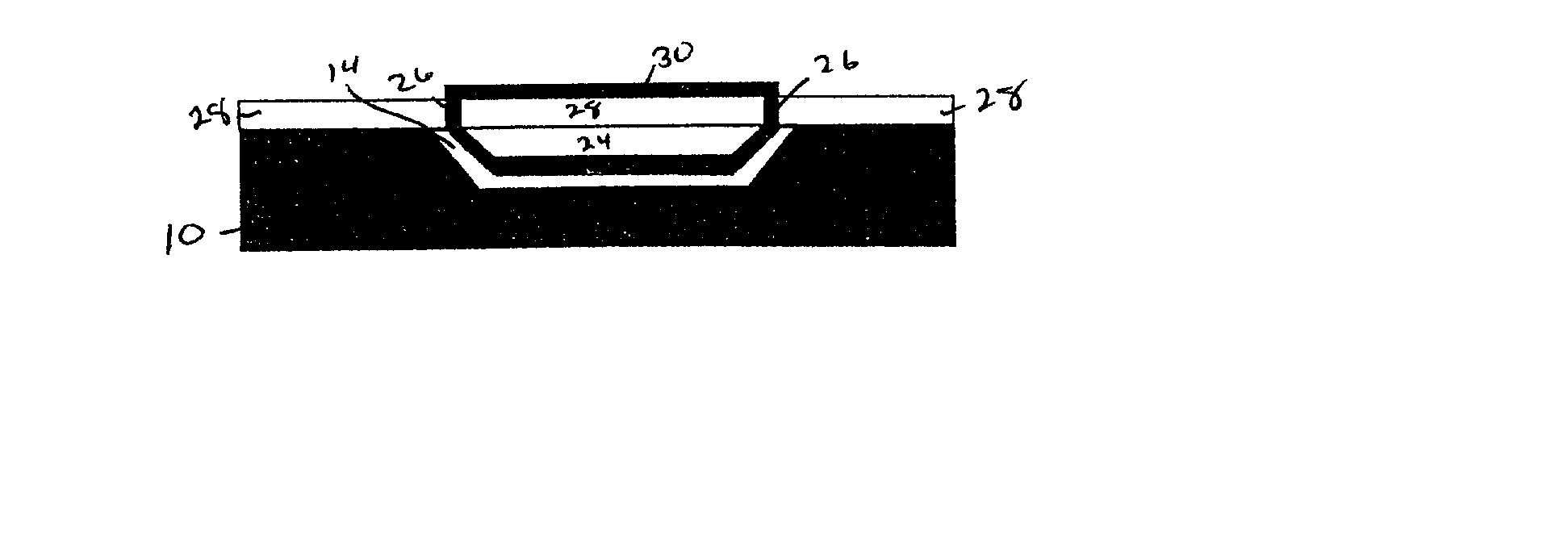
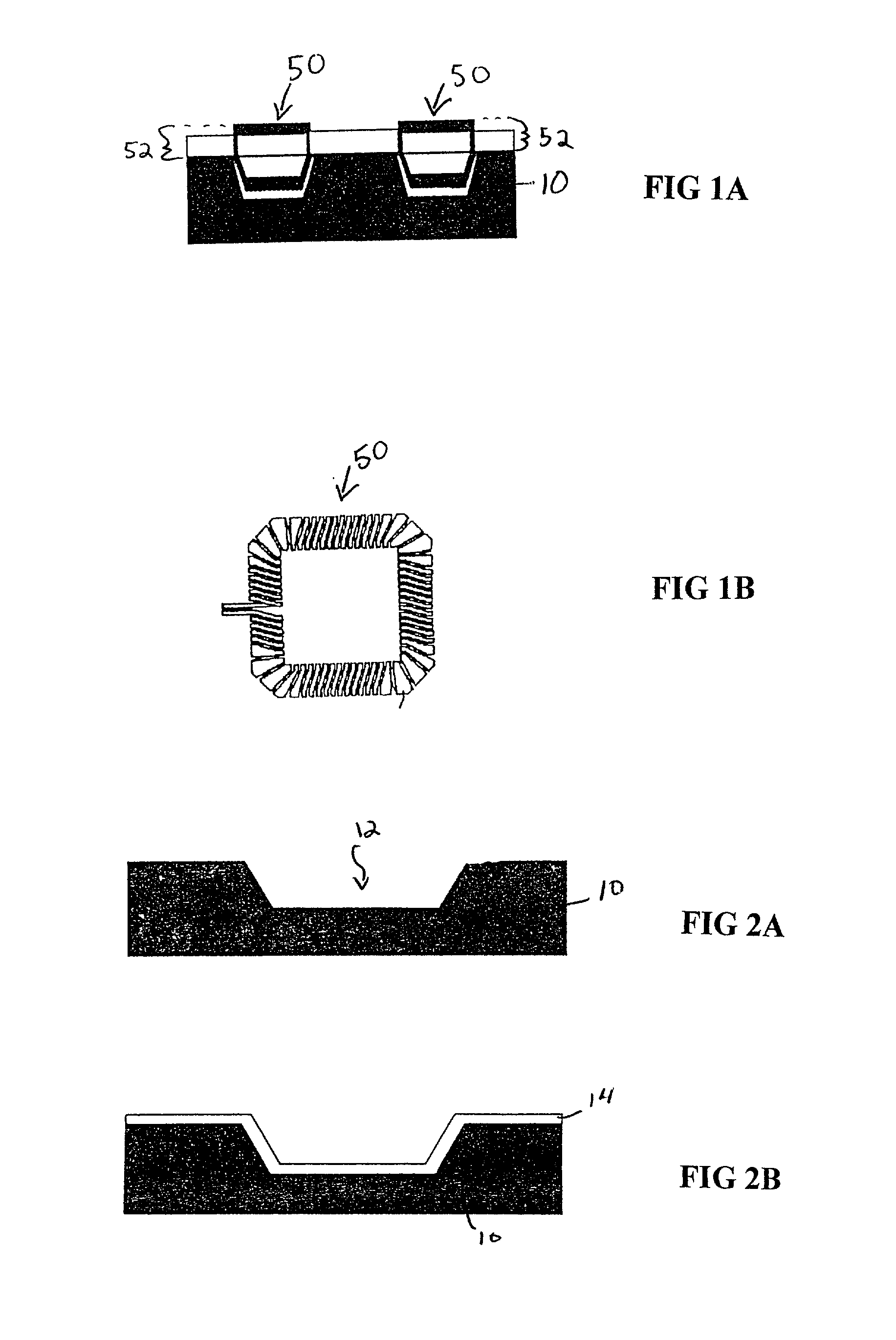
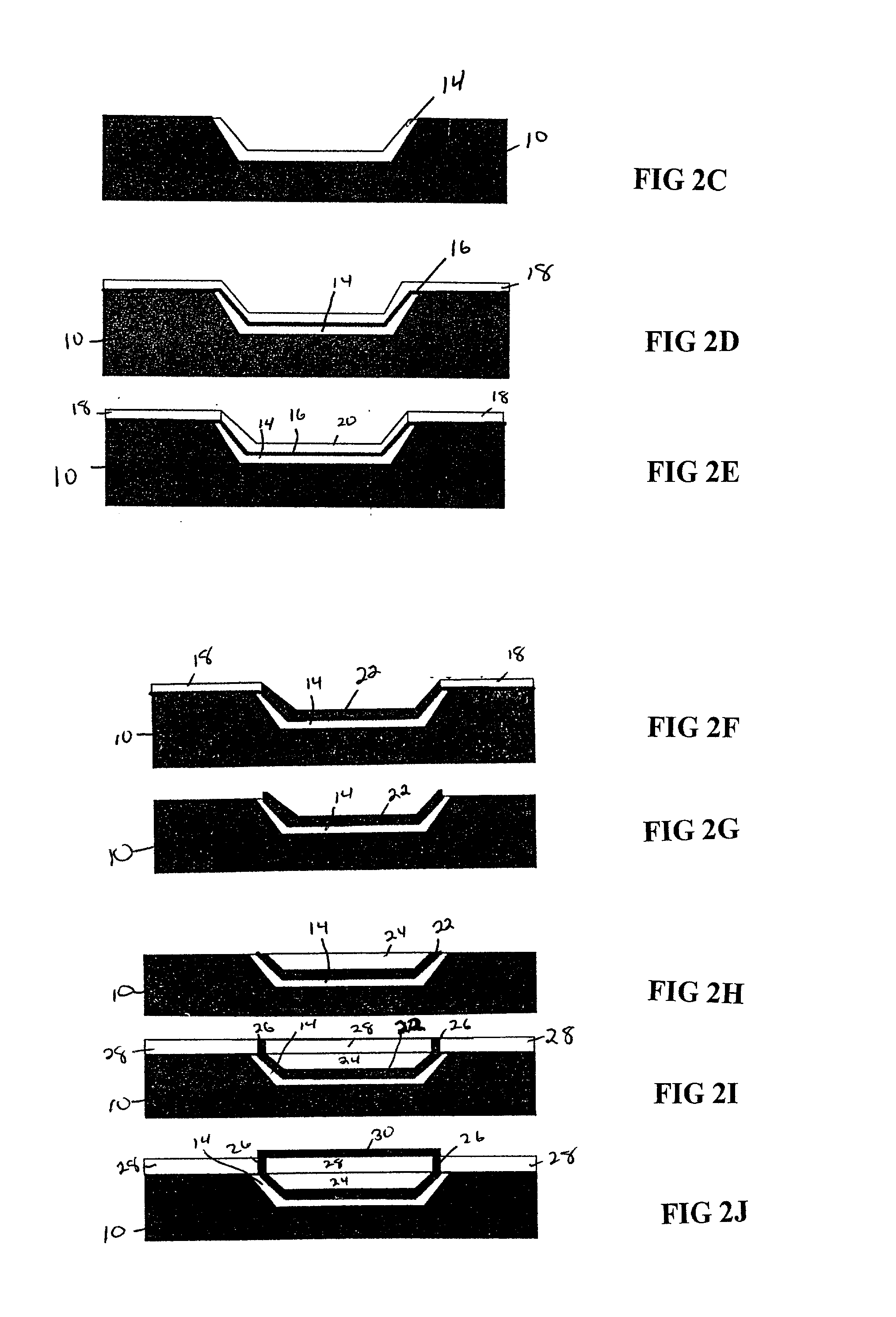
[0027] Reference is first made to FIGS. 1A (cross-sectional view) and 1B (top view) which illustrate the inventive semiconductor structure. Specifically, FIG. 1A comprises a structure that includes substrate 10 having one or more solenoidal coils 50 formed inside cavities that are formed in the substrate and partially in BEOL wiring levels 52. A top view of solenoidal coils 50 of FIG. 1A is shown, for example, in FIG 1B.

[0028] In accordance with the present invention, each solenoidal coil 50 includes bottom coil element 22 and top coil element 30 that are in electrical contact with each through side co...


PUM


Abstract

A means for fabrication of solenoidal inductors integrated in a semiconductor chip is provided. The solenoidal coil is partially embedded in a deep well etched into the chip substrate. The non-embedded part of the coil is fabricated as part of the BEOL metallization layers. This allows for a large cross-sectional area of the solenoid turns, thus reducing the turn-to-turn capacitive coupling. Because the solenoidal coils of this invention have a large diameter cross-section, the coil can be made with a large inductance value and yet occupy a small area of the chip. The fabrication process includes etching of a deep cavity in the substrate after all the FEOL steps are completed; lining said cavity with a dielectric followed by fabrication of the part of the coil that will be embedded by deposition of a conductive material metal through a mask; deposition of dielectric and planarization of same by CMP. After planarization the fabrication of the remaining part of the solenoidal coil is fabricated as part of the metallization in the BEOL (i.e. as line/vias of the BEOL). To further increase the cross section of the solenoidal coil part of it may be built by electrodeposition through a mask on top of the BEOL layers.

Description

FIELD OF THE INVENTION[0001] The present invention relates to semiconductor devices, and more particularly to a multiturn solenoidal inductor integrated in a semiconductor chip, such as those used for radio frequency (RF) communications. The present invention also relates to a method of fabricating the inventive multiturn solenoidal inductor.BACKGROUND OF THE INVENTION[0002] Inductors integrated in semiconductor chips are normally fabricated in the shape of spirals in one BEOL (back-end-of-the-line) metallization level (plus vias to connect to and from the return arm). Because of the limited thickness of BEOL metallization layers (on the order of about 2 to about 4 microns), spiral inductors have a relatively high resistance (on the order of about 1-5 ohms or greater) for a given inductance value. Dual metal layers, with interconnecting vias, are sometimes utilized to reduce the spiral resistance. Because the inductance value is directly related to the length of the inductor trace, ...

Claims


Application Information

Patent Timeline
IPC IPC(8): H01F17/00H01F17/04H01F17/06H01F27/00H01F27/06H01F41/04H01L21/02H01L27/08
CPCH01F17/0006H01F17/0033H01F41/041H01L27/08H01L28/10H01L27/04H01L29/00
Inventor ACOSTA, RAUL E.CARASSO, MELANIE L.CORDES, STEVEN A.GROVES, ROBERT A.LUND, JENNIFER L.ROSNER, JOANNA
Owner GLOBALFOUNDRIES US INC
Why Eureka
Try Eureka