Semiconductor package with lead frame

a technology of semiconductor and lead frame, which is applied in the direction of semiconductor/solid-state device details, semiconductor devices, electrical apparatus, etc., can solve the problems of increasing the length of those passages, and achieve the effects of improving bonding strength, reducing the occurrence of cracking of semiconductor packages, and reducing the cracking ra

Inactive Publication Date: 2002-09-19
AMKOR TECH SINGAPORE HLDG PTE LTD
View PDF0 Cites 21 Cited by
  • Summary
  • Abstract
  • Description
  • Claims
  • Application Information

AI Technical Summary

Benefits of technology

0009] In accordance with the present invention, there is provided a semiconductor package including a lead frame and an encapsulation portion or sealing part which is formed on a prescribed region of the lead frame. The lead frame of the present semiconductor package is formed to have a thin profile so as to minimize occurrences of the cracking of the semiconductor package during the process of manufacturing the same, which typically involves the completion of a singulation process or step. Additionally, in the present semiconductor package, the contact area between the sealing part and the lead frame is maximized to improve the bonding strength between the lead frame and the

Problems solved by technology

Further, the lead frame and the sealing part are sized and configured relative to each other such that the increased contact area between them als

Method used


Image

  • Semiconductor package with lead frame
  • Semiconductor package with lead frame
  • Semiconductor package with lead frame

Examples


first embodiment

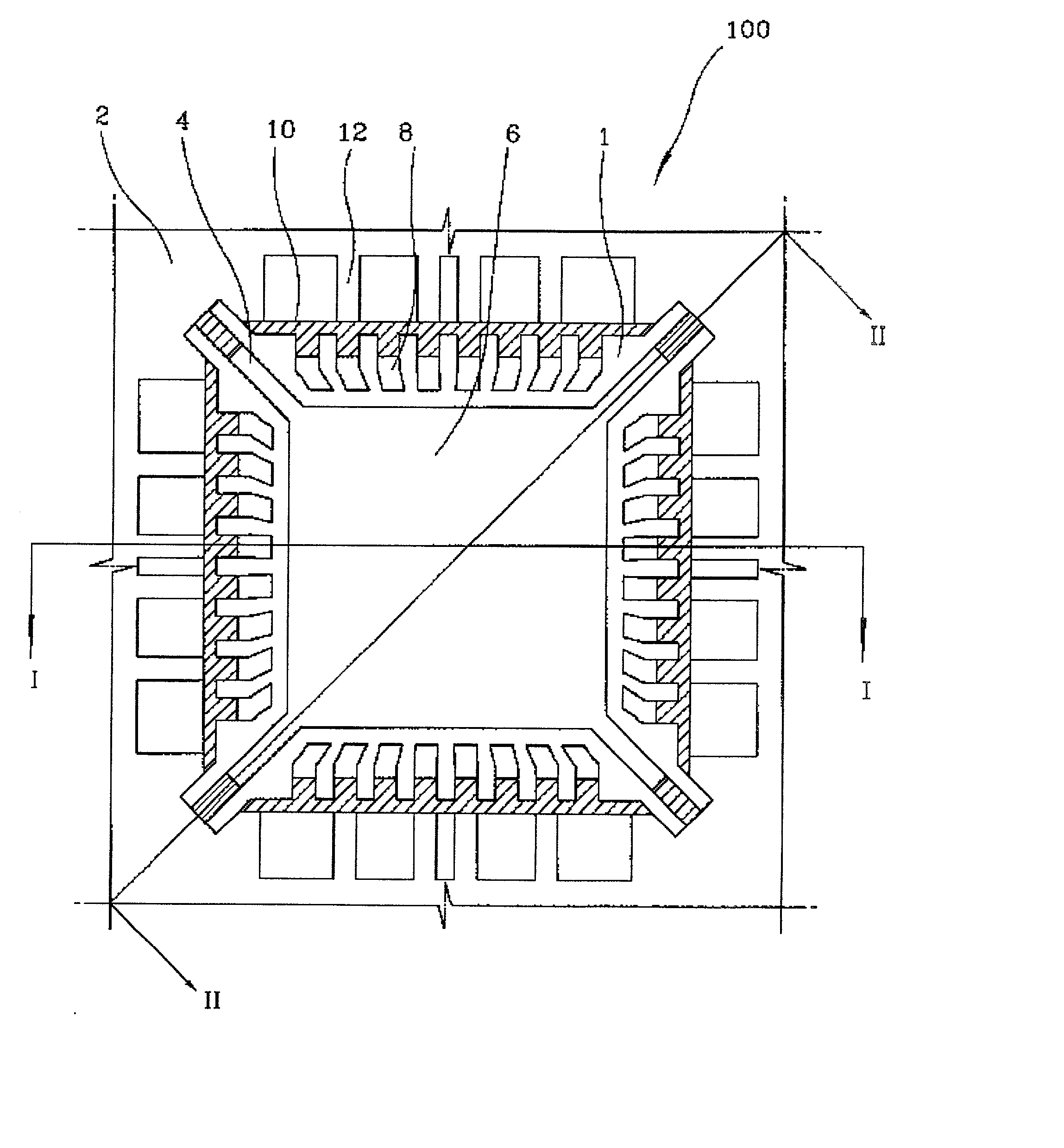
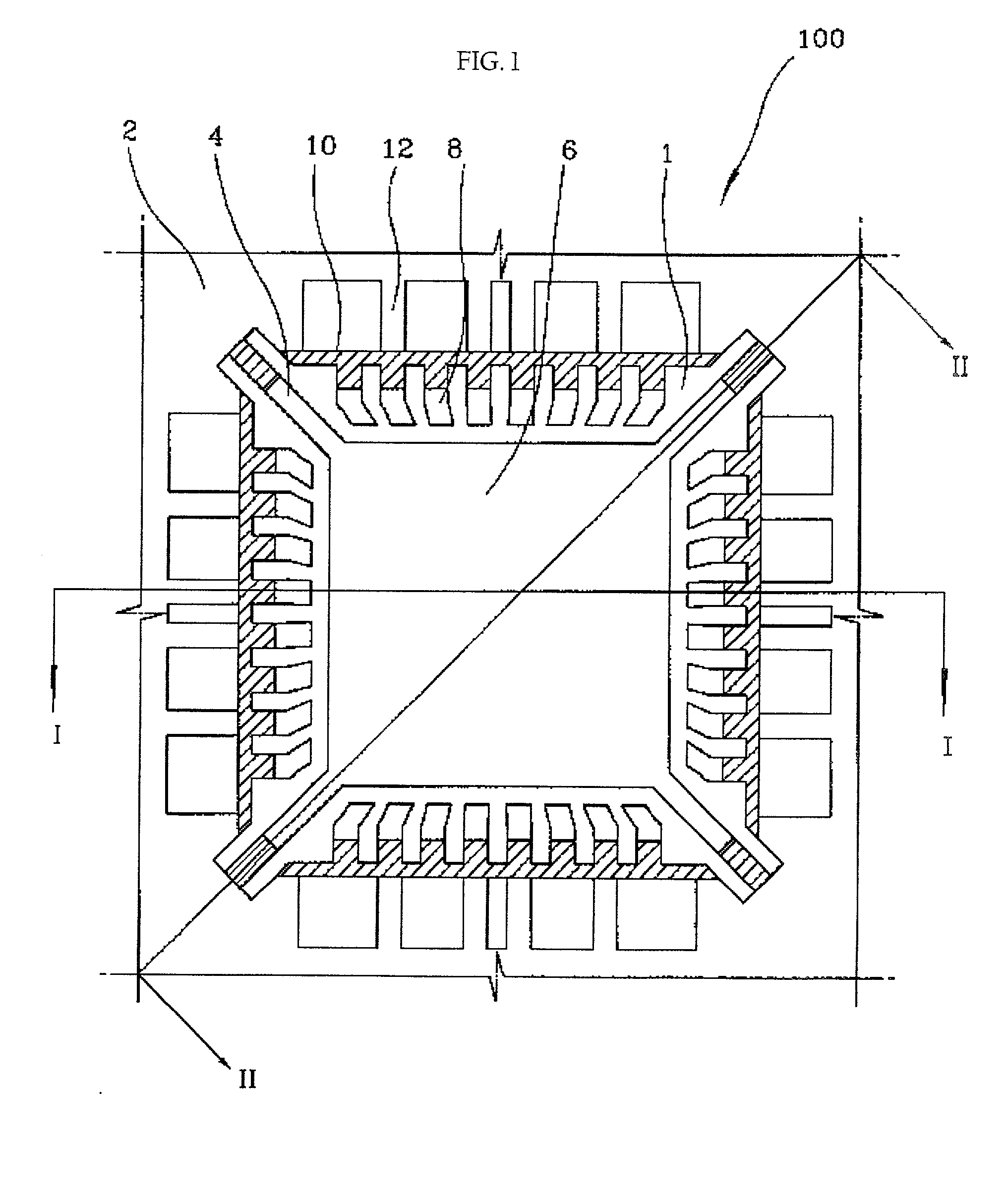
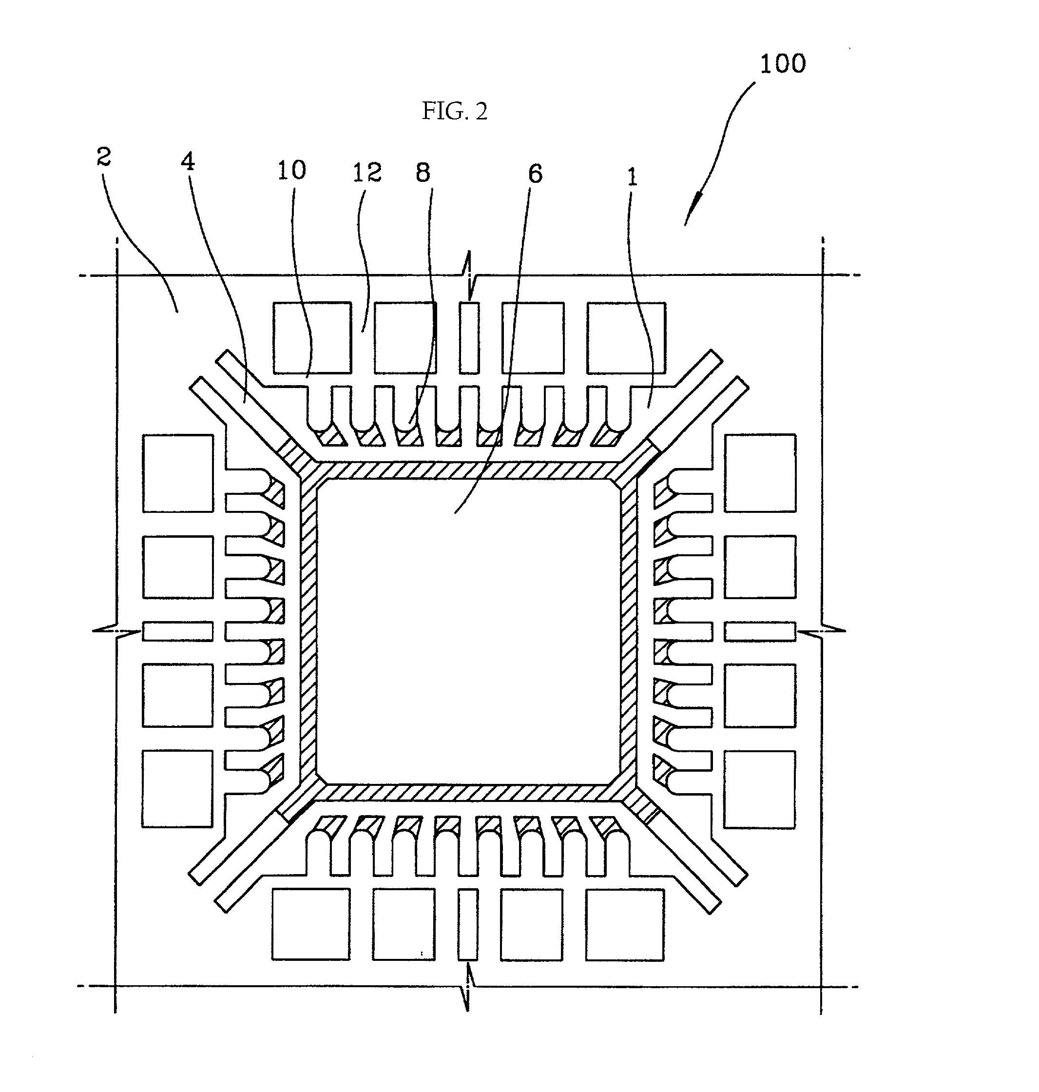
[0029] Referring now to the drawings wherein the showings are for purposes of illustrating preferred embodiments of the present invention only, and not for purposes of limiting the same, FIGS. 1 and 2 depict top and bottom plan views, respectively, of a lead frame 100 for use in a semiconductor package 200 constructed in accordance with the present invention. Lead frames for semiconductor packages are typically manufactured by mechanically stamping or chemically etching a continuous metal strip. The lead frame serves as a lead connecting a semiconductor chip to an external circuit such as a motherboard. The lead frame further serves as a frame for fixing the semiconductor package to the motherboard while providing an electrical connection between the motherboard and the semiconductor chip.

[0030] The lead frame 100 of the present invention comprises a frame 2 which is a substantially flat or planar plate defining a centrally located space 1. Disposed within the space 1 is a chip moun...

second embodiment

[0050] Referring now to FIG. 11, there is shown a semiconductor package 201 constructed in accordance with the present invention. The primary distinction between the semiconductor package 201 and the aforementioned semiconductor package 200 lies in the increased thickness of the sealing part 28 formed on the fourth surfaces 8d of the leads 8 in the semiconductor package 201. As seen in FIG. 13, each lead 8 has a thickness t1 from the second surface 8b to the fourth surface 8d, and a thickness t2 from the first surface 8a to the third surface 8c. The thickness from the fourth surface 8d of each lead 8 to the upper surface of the sealing part 28 is defined as t3. The thickness t3 exceeds the thickness t2 and the thickness t1. In this regard, the criticality is that the thickness t3 be selected such that the upper surface of the sealing part 28 formed on the fourth surface 8d of each of the leads 8 is positioned or disposed at a level which is higher than that of the first surface 8a o...

third embodiment

[0053] Thus, in the semiconductor package 202 of the third embodiment, the sealing part 28 formed on the first surface 8a of each of the leads 8 is in direct contact with the lower tool 42 during the singulation process, thus allowing the sealing part 28 to absorb the impact of the punch 43. This attribute also substantially prevents occurrences of cracking in the semiconductor package periphery 202 during the manufacture thereof.

[0054] As discussed above, in each of the embodiments of the semiconductor package 200, 201, 202, the contact area between the sealing part 28 and the singulated portions of the lead frame 100 is increased, thus having the effect of improving the bonding strength between the lead frame 100 and the sealing part 28. This increased contact area between the sealing part 28 and the lead frame 100 also maximizes the passage length for potential moisture permeation, thereby minimizing such moisture permeation potential. Further, in the semiconductor packages 200, ...


PUM


Abstract

A semiconductor package including a sealing part which is bonded to a lead frame. The lead frame is formed to include portions of reduced thickness for purposes of providing maximum crack prevention during a singulation process involved in the manufacture of the semiconductor package. Additionally, the lead frame and the sealing part are sized and configured relative to each other so as to maximize the contact area therebetween, thus having the effect of improving the bonding strength between the lead frame and the sealing part. This increased contact area between the sealing part and the lead frame also maximizes the lengths of those passages susceptible to moisture permeation, thus minimizing such moisture permeation potential.

Description

CROSS-REFERENCE TO RELATED APPLICATIONS[0001] The present application claims priority to Korean Patent Application Nos. 2001-14140 filed Mar. 19, 2001 and 2001-18336 filed Apr. 6, 2001.STATEMENT RE: FEDERALLY SPONSORED RESEARCH / DEVELOPMENT[0002] (Not Applicable)BACKGROUND OF THE INVENTION[0003] 1. Field of the Invention[0004] The present invention relates generally to semiconductor packages, and more particularly to a semiconductor package which is sized and configured to, among other things, optimize the bonding strength between the lead frame and the remainder of the package, prevent moisture permeation into the package, and minimize cracking of the package during the process of manufacturing the same.[0005] 2. Description of the Related Art[0006] The current trend in the electronics industry is to provide electronic appliances which are multifunctional, compact, and capable of achieving high performance levels. In view of this trend, a requirement has arisen that the semiconducto...

Claims


Application Information

Patent Timeline
IPC IPC(8): H01L21/56H01L23/00H01L23/31H01L23/495
CPCH01L21/565H01L23/3107H01L23/49548H01L23/564H01L2224/32245H01L2224/48091H01L2224/48247H01L2224/73265H01L2924/01046H01L2924/01078H01L2924/01079H01L2924/1815H01L2924/00014H01L24/48H01L2224/45124H01L2924/181H01L2924/00012H01L2224/05599H01L2224/45144H01L2224/45147H01L24/45H01L2924/18301
Inventor JEONG, JUNG HOHONG, JONG CHULKIM, EUN DEOK
Owner AMKOR TECH SINGAPORE HLDG PTE LTD
Why Eureka
Try Eureka