Optical semiconductor module and light amplifier

a technology of optical semiconductor modules and light amplifiers, applied in the direction of optical elements, instruments, semiconductor/solid-state device details, etc., can solve the problems of difficult to arrange an isolator in the optical system of the optical module, the oscillation wavelength of the optical semiconductor element is set to a considerably unstable state, and the oscillation wavelength of the laser beam in the optical semiconductor element is difficult to stabilize, so as to achieve high saturation output power and low noise figure

Inactive Publication Date: 2002-09-19
MITSUBISHI ELECTRIC CORP
View PDF6 Cites 10 Cited by
  • Summary
  • Abstract
  • Description
  • Claims
  • Application Information

AI Technical Summary

Benefits of technology

0030] Therefore, by using the optical semiconductor module according to one of the first to eighth inventions for the optical amplifier, an optical amplifier having a high saturation output power and a low noise figure can be obtained.

Problems solved by technology

In this case, because a high light output power is required of the optical module, it is difficult to arrange an isolator in the optical system of the optical module.
In cases where no isolator can be arranged in the optical system, because a reflected laser beam occurring in the optical semiconductor module or on the outside of the optical semiconductor module is again incident on the optical semiconductor element as a returned laser beam, it is well known that the oscillation wavelength of the optical semiconductor element is set to a considerably unstable state.
However, in case of the use of an optical semiconductor module having a low coupling efficiency such as the optical system of the conventional optical semiconductor module, unless a reflectance of the fiber grating of the optical fiber is heightened, it is impossible to stabilize the oscillation wavelength of the laser beam in the optical semiconductor element.
Also, in case of the use of a light amplifier, because an optical semiconductor module having a low coupling efficiency and a low light output power is used, a gain in the light amplifier is decreased, and a noise figure in the light amplifier is increased.
Therefore, it is difficult to sufficiently obtain excellent characteristics of the light amplifier.

Method used


Image

  • Optical semiconductor module and light amplifier
  • Optical semiconductor module and light amplifier
  • Optical semiconductor module and light amplifier

Examples


embodiment 1

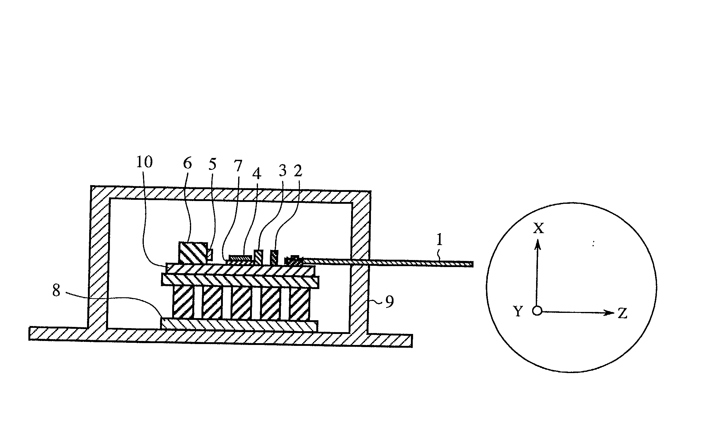
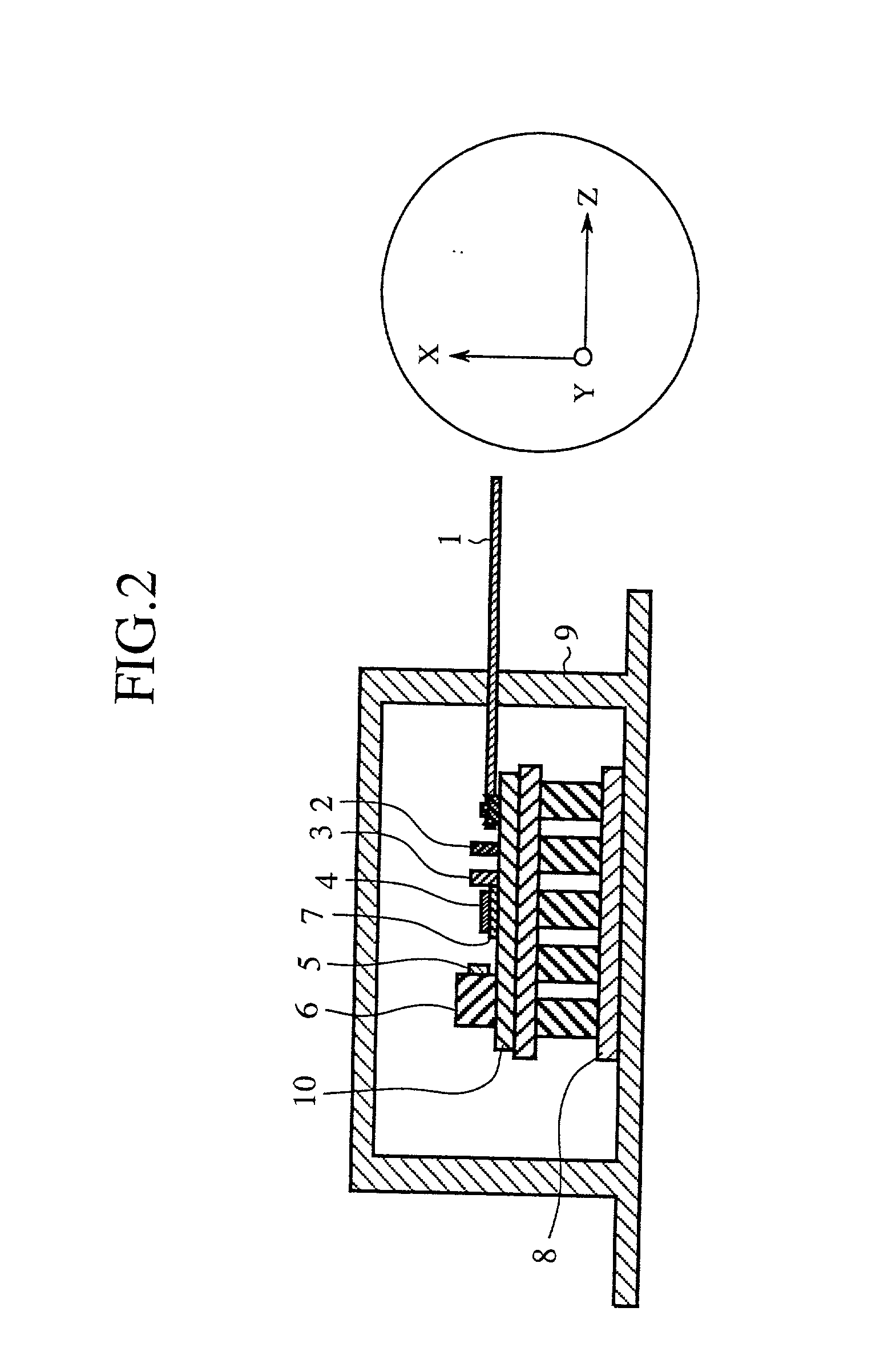
[0040] FIG. 2 is a schematic view showing an optical semiconductor module according to a first embodiment of the present invention. In FIG. 2, 1 indicates an optical fiber. 2 indicates a second lens. 3 indicates a first lens. 4 indicates an optical semiconductor element. 5 indicates a monitoring photo diode (PD). 6 indicates a PD carrier. 7 indicates a sub-mount. 8 indicates a Peltier cooler. 9 indicates a hermetic package. 10 indicates a chip carrier.

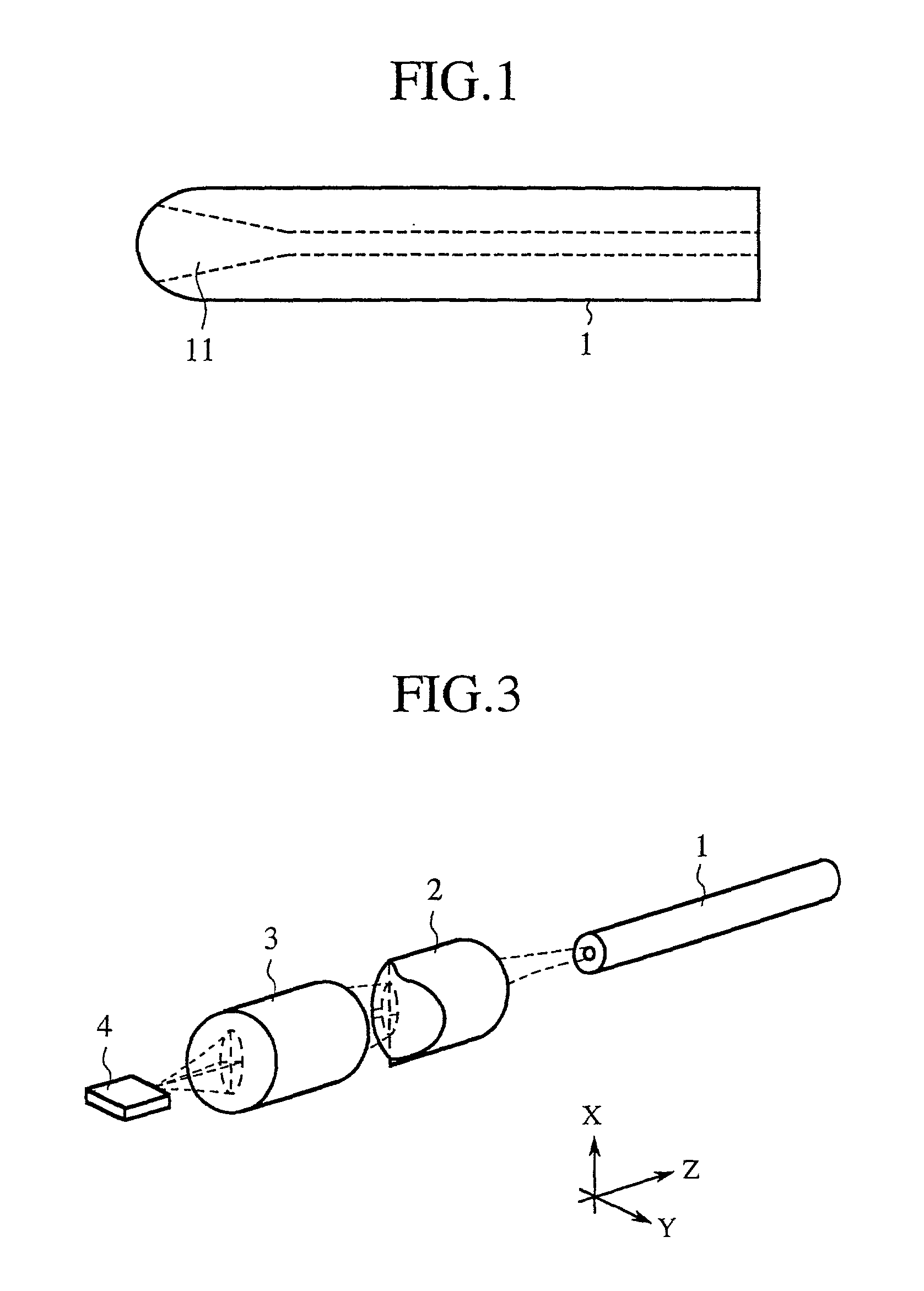
[0041] FIG. 3 is a constitutional view of an optical system picked up from the optical semiconductor module of the first embodiment of the present invention. FIG. 4 is an explanatory view showing a radiation pattern of a laser beam radiated from the optical semiconductor element 4. In FIG. 4, 12 indicates a mode field. 13 indicates a far field. The optical semiconductor element 4 has the mode field 12 lengthened in the lateral direction. Because of the shape of the mode field 12, the far field 13 is formed in a shape lengthened in a lo...

embodiment 2

[0046] In the first embodiment, a lens system composed of the first lens 3 and the second lens 2 is arranged in the optical semiconductor module. In this case, a coupling optical system is complicated, and the number of optical elements and the number of steps of the assembling work are increased. The complication of the coupling optical system and the increase of both the optical elements and the assembling work influence on the assembling precision of the optical semiconductor module. To prevent these problems, in a second embodiment, the second lens 2 is tightly attached to the optical fiber 1 by using a bonding agent, or the second lens 2 is tightly attached to the optical fiber 1 according to a melting method. Therefore, the number of optical elements is decreased, and the assembling work can be easily performed. In addition, as is described in the first embodiment, it is not required to process the second lens 2 with high processing precision. Therefore, even though the second...

embodiment 3

[0048] As is described in the second embodiment, the optical fiber 1 and the second lens 2 are connected with each other in a third embodiment. In cases where a refractive index of the core of the optical fiber 1 differs from that of the second lens 2, Fresnel reflection of the laser beam necessarily occurs on an end face of the optical fiber 1. In cases where the optical semiconductor element 4 is formed of a semiconductor laser, because the laser beam reflected on the end face of the optical fiber 1 is returned to the semiconductor laser, oscillation conditions in the semiconductor laser are made unstable. For example, an optical fiber often used for an optical connector is processed according to a physical contact (PC) polishing, and a maximum value of a reflectance of the optical fiber is equal to -40 dB. Therefore, to obtain a reflectance of -40 dB in the optical fiber 1, it is required to set a difference in refractive index between the second lens 2 and the core of the optica...


PUM


Abstract

A first lens and a second lens are used in an optical semiconductor module, an entrance plane of the second lens is formed in a cylindrical shape. Accordingly, an optical semiconductor module can be obtained by changing a mode field of an optical fiber to an elliptically-shaped apparent mode field by using the second lens so as to be possible to efficiently couple a laser beam radiated from an optical semiconductor element with the optical fiber.

Description

[0001] This application is based upon and claims priority from U.S. patent application Ser. No. 09 / 958,657, the entire contents of which are incorporated herein by reference. U.S. Patent Application Ser. No. 09 / 958,657 is the national phase under 35 U.S.C. .sctn.371 of PCT International Application No. PCT / JP01 / 01527 which has an International filing date of Feb. 28, 2001, which designated the United States of America and was not published in English.TECHNICAL FIELD[0002] The present invention relates to an optical semiconductor module in which a laser beam radiated from a light emitting device such as a semiconductor laser is coupled with an optical fiber, and the present invention relates to a light amplifier in which the optical semiconductor module is used as an excitation light source.BACKGROUND ART[0003] As an optical system of a conventional laser diode module for optical communication, "Optical Module" is disclosed in Published Unexamined Japanese Patent Application No. H11-...

Claims


Application Information

Patent Timeline
Patent Type & Authority Applications(United States)
IPC IPC(8): G02B6/32G02B6/42
CPCG02B6/32G02B6/4206
Inventor ONODERA, TAKAYUKISAKAI, KIYOHIDE
Owner MITSUBISHI ELECTRIC CORP
Why Eureka
Try Eureka