

Method and apparatus for the determination of mask rules using scatterometry
a scatterometry and mask rule technology, applied in the field of mask rule determination methods and apparatuses, can solve the problems of fracturing the wafer and the cd-sem preparation process, affecting the output data set, and the prior art method of making this determination is extremely expensive, time-consuming and destructive,
- Summary
- Abstract
- Description
- Claims
- Application Information
AI Technical Summary
Benefits of technology
Problems solved by technology
Method used
Image

Examples
Embodiment Construction
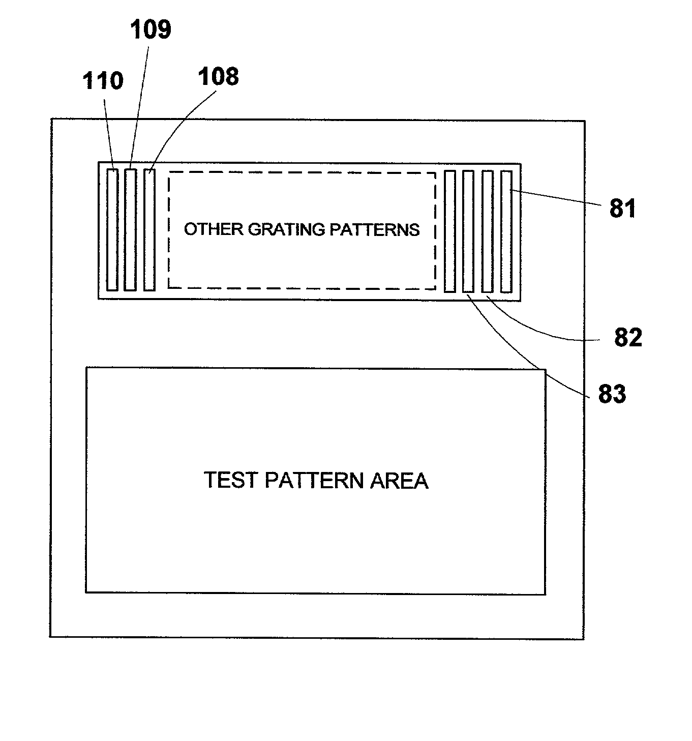
[0066] A second preferred embodiment is shown by reference to FIG. 18. In the second preferred embodiment grating patterns 81 through 110 are replaced by bi-periodic grating patterns. Bi-periodic grating pattern 140 with OPC correction lines 142 is shown in FIG. 18. Bi-periodic grating pattern 140 is referred to as being a bi-periodic grating because there are two repeating pitches throughout the grating. The first pitch refers to the pitch distance between adjacent lines within each group 170, 180 and 190. The second pitch refers to the pitch distance between adjacent groups. Applicants have shown through simulation that by diffracting light off gratings created by a bi-periodic grating pattern, the user can better ascertain the profile of each line within the group if the scatterometry library is created using the robust RCWA technique implemented in the ODP technique described in the background section. For example, in groups 170, 180 and 190 there is a first line 150. This line ...
PUM
| Property | Measurement | Unit |
|---|---|---|
| side wall angles | aaaaa | aaaaa |
| side wall angle | aaaaa | aaaaa |
| distance | aaaaa | aaaaa |
Abstract
Description
Claims
Application Information