

Method of manufacturing optical devices and related improvements
- Summary
- Abstract
- Description
- Claims
- Application Information
AI Technical Summary
Benefits of technology
Problems solved by technology
Method used
Image

Examples
Embodiment Construction
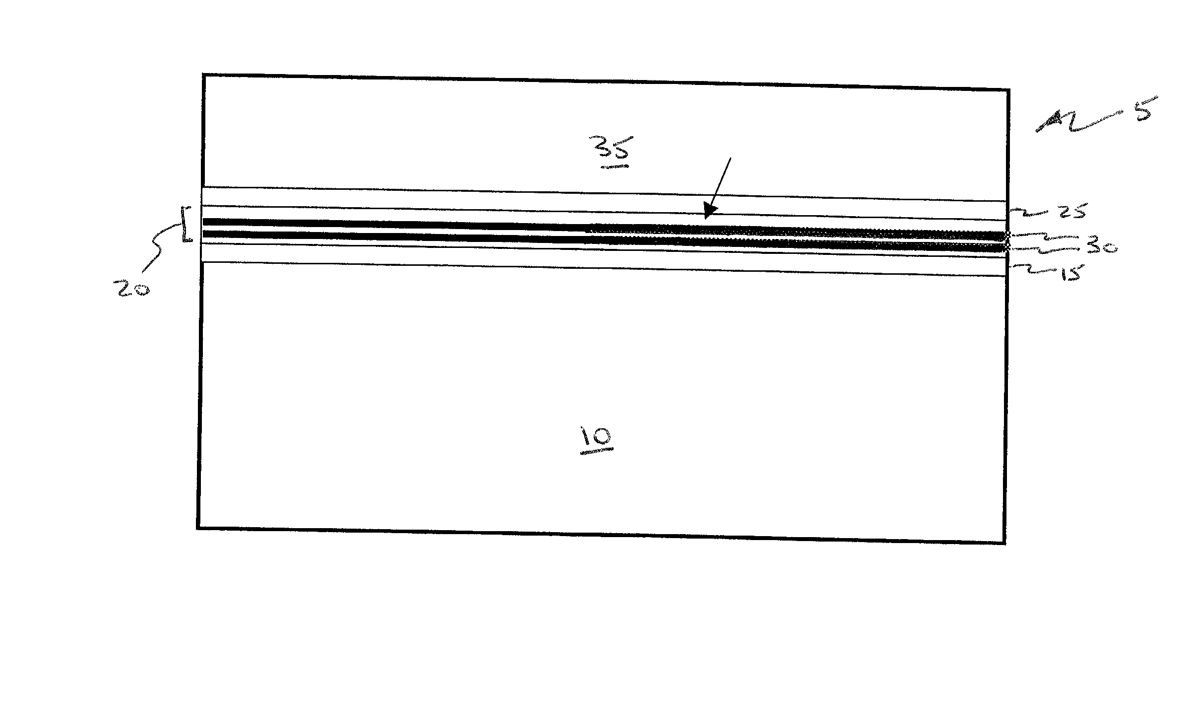
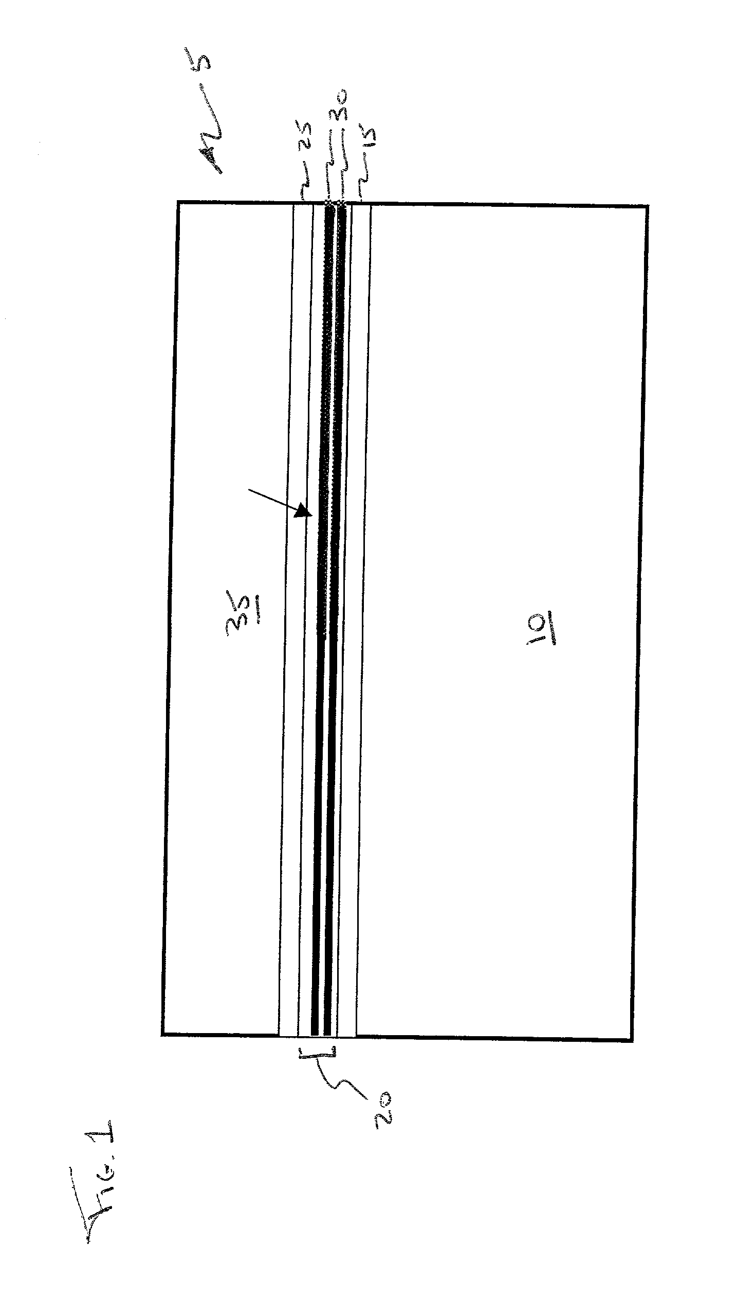
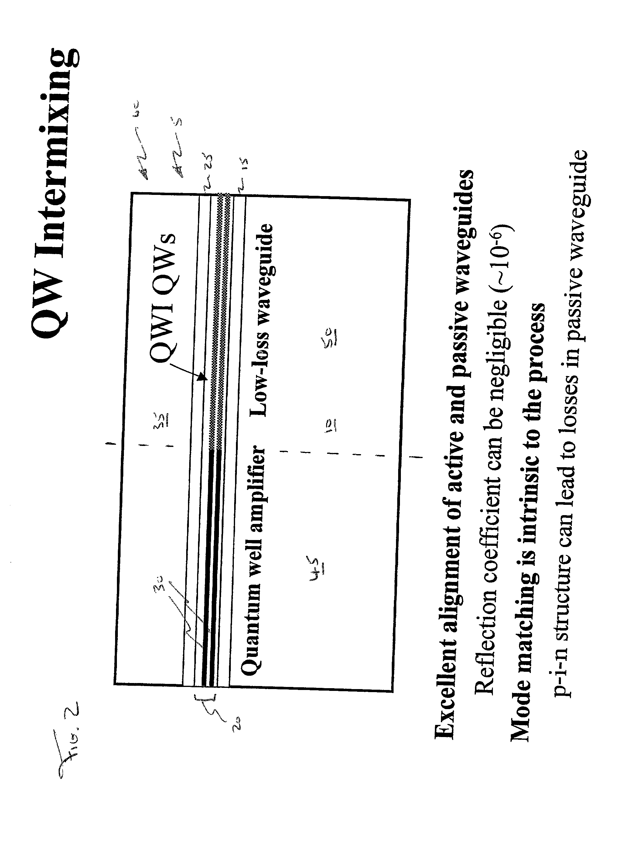
[0082] There now follows an example which illustrates a typical band-gap shift which can be obtained using IFVD in a method of manufacturing an optoelectronic device according to the present invention in a long wavelength aluminium alloy such as Indium Aluminium Gallium Arsenide (GaAs) Arsenide, (InAlGaAs), grown on an Indium Phosphide (InP) substrate.
[0083] The dielectric layer 51 deposition requires a sputter chamber 70 configured in a diode configuration with a cathode / anode (plate) separation of the order to 100 mm. The cathode 80 and anode 85 are each configured as substantially four inch circular plates. The gas used in this example for sputter deposition is typically Argon, but other suitable inert gases may be used, and also small amounts of Oxygen may be added to the Argon Plasma 86, eg approximately 10% by volume, to improve the stoichiometry of the deposited dielectric layer 51. The dielectric material used in the method is typically Silica (SiO.sub.2), but other dielectr...
PUM
 Abstract
Description
Claims
Application Information