
Mounting structure and mounting method of a photovoltaic element, mounting substrate for mounting a semiconductor element and method for mounting said semiconductor element on said mounting substrate

a technology of photovoltaic elements and mounting structures, which is applied in the direction of photovoltaic supports, pv power plants, transistors, etc., can solve the problems of high cost of photovoltaic elements, material cost of solar cells (the photoelectric conversion elements) constituting solar cells, and the cost of retaining substrates on which the photovoltaic elements are mounted is expensive to be similar to or more than the cost of the photovoltaic elemen

Inactive Publication Date: 2002-10-03
CANON KK
View PDF18 Cites 43 Cited by
  • Summary
  • Abstract
  • Description
  • Claims
  • Application Information

AI Technical Summary

Benefits of technology

[0039] In this mounting structure, the metal body is capable of being a heat spreader which has a heat radiation function And the metal body makes it possible to readily output a large electric current.
[0043] The semiconductor element-mounting substrate thus structured is greatly advantageous in that even when the semiconductor element mounted is a thin type photovoltaic element which is used under condition with irradiation of a highly condensed light, the mounting substrate makes it possible to desirably mount said photovoltaic element thereon without displacing the originally arranged position of said photovoltaic element and while preventing the cream solder material or / and the flux contained the rein from depositing on the light receiving face of the photovoltaic element.

Problems solved by technology

However, for the atomic power generation, there are problems that are difficult to be solved, such as radioactive wastes and the like which cause air pollution.
For any of these solar cells, the material cost of the cell (the photoelectric conversion element) constituting the solar cell accounts for the largest rate of the cost of the solar cell.
However, in the prior art as described in the above, there are disadvantages as will be described below.
In the method of mounting the photovoltaic element which has explained with reference to FIGS. 16(A)-16(D) and FIGS. 17(A)-17(C), there is a disadvantage in that the retaining substrate on which the photovoltaic element is mounted is costly to be similar to or more than the cost of the photovoltaic element and this makes it difficult to reduce the production cost of the optical-concentration type solar cell module.
There is also a disadvantage in that the method comprises the step of mounting the photovoltaic element on the retaining substrate and the step of joining the retaining substrate having the photovoltaic element mounted thereon with the heat sink by means of the silver paste, each of these steps including the heating step, and each of these steps takes a time until the step is completed, and therefore, this unavoidably raises the production cost of the optical-concentration type solar cell module.
Further, in the case where the circuit board as the retaining substrate comprises a circuit board made of a ceramic, there is an occasion in that the ceramic layer in the ceramic circuit board is cracked due to the repetition of the heat treatment.
This entails problems such that the heat of the photovoltaic element is not sufficiently radiated, and as a result, the temperature of the photovoltaic element is increased to cause a reduction in the power generation efficiency and the photovoltaic element is sometimes deteriorated in terms of the performance.
Besides, in this case, there is considered occurrence of fusion in the solder which joins the photovoltaic element with the circuit board.
Other than the above-described disadvantages, there is also a disadvantage in that batch processing is necessitated because the components are separately supplied and therefore, it is necessary to use a prescribed fabrication apparatus for the batch processing, which is relatively costly
Additionally, for the foregoing method of mounting the photovoltaic element, there are other disadvantages as will be described below.
In this case, a problem is liable to occur in that the resist formed on the circuit board suffers from extreme heat deterioration or it is thermally decomposed to disappear.
In addition, when the resist is thermally decomposed, foreign matter is generated to deposit on the light receiving face of the photovoltaic element.
Therefore, the method in that the resist is formed on the circuit board is not always effective.

Method used


Image

  • Mounting structure and mounting method of a photovoltaic element, mounting substrate for mounting a semiconductor element and method for mounting said semiconductor element on said mounting substrate
  • Mounting structure and mounting method of a photovoltaic element, mounting substrate for mounting a semiconductor element and method for mounting said semiconductor element on said mounting substrate
  • Mounting structure and mounting method of a photovoltaic element, mounting substrate for mounting a semiconductor element and method for mounting said semiconductor element on said mounting substrate

Examples


examples 1 to 5

OF THE FIRST ASPECT OF THE PRESENT INVENTION

example 1

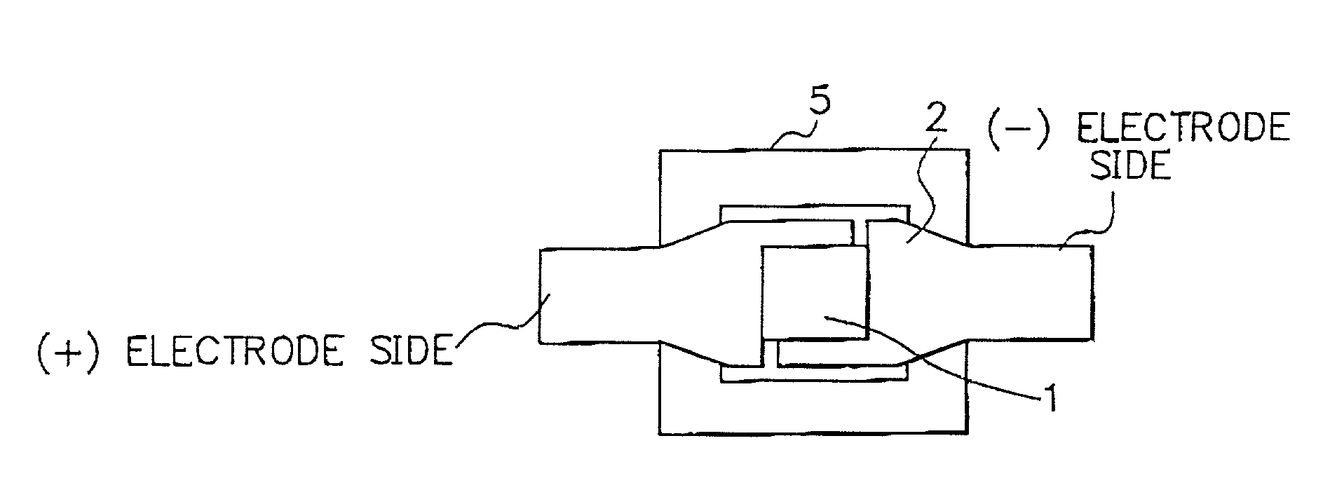
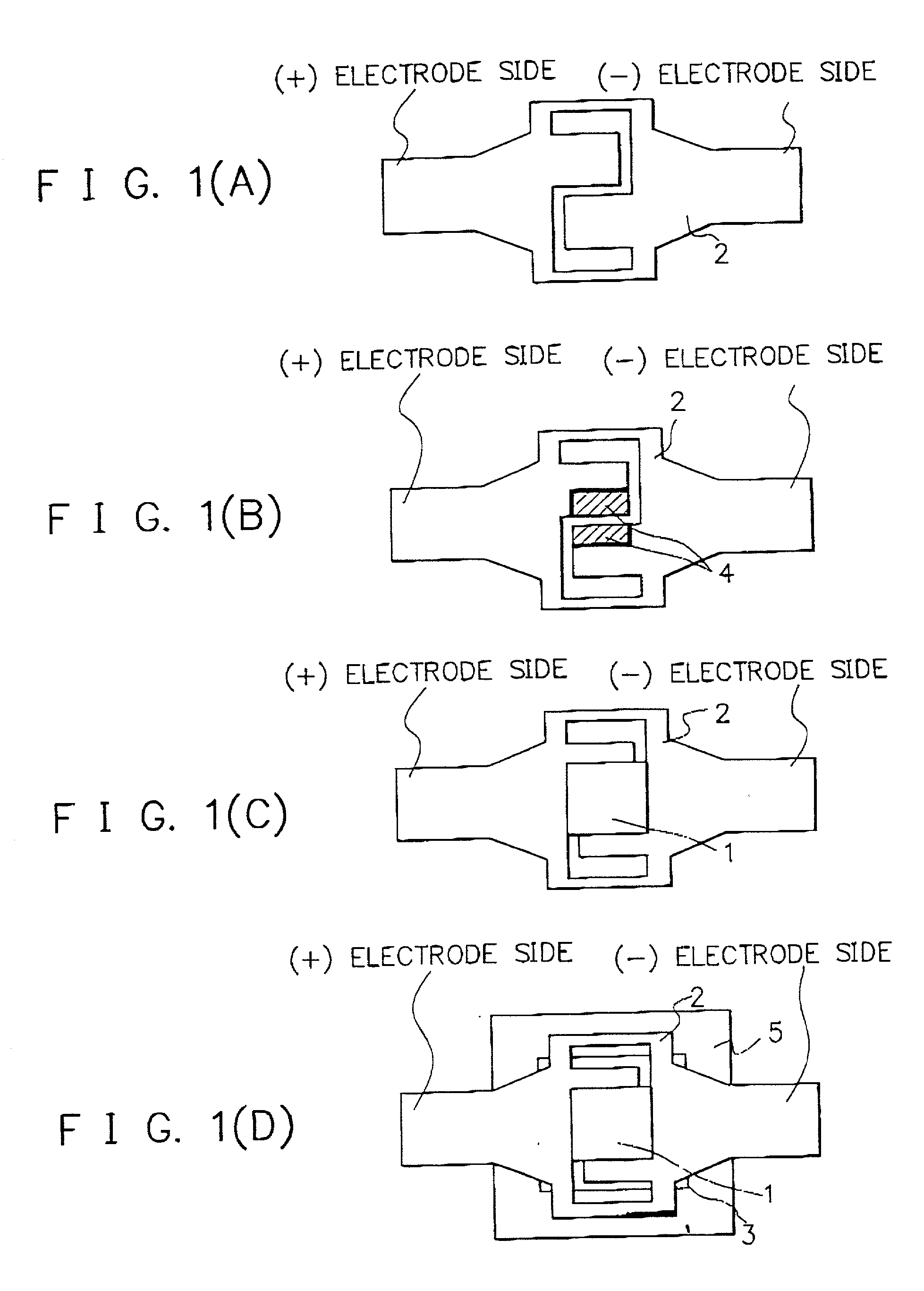
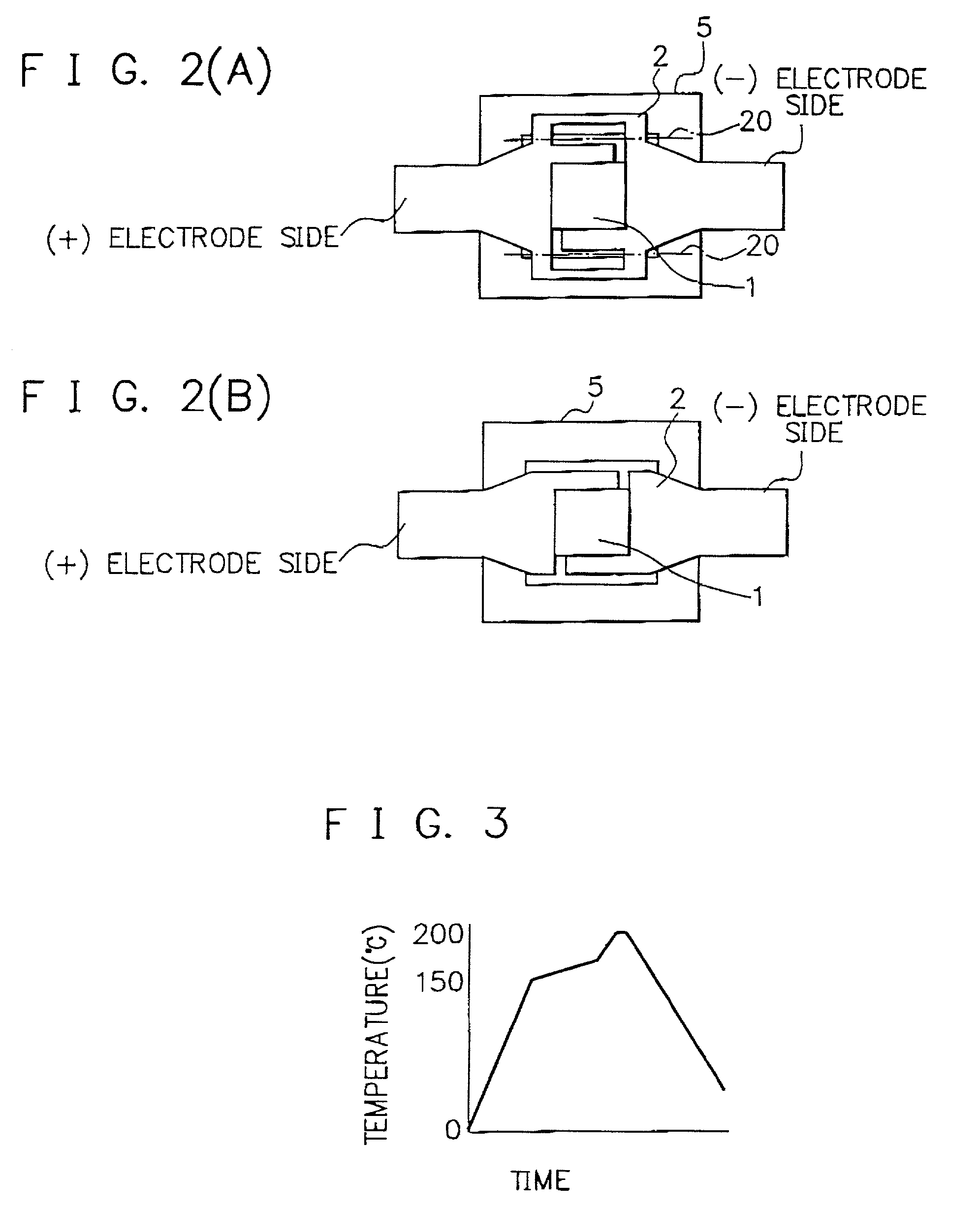
[0157] FIGS. 1(A) to 1(D) and FIGS. 2(A) and 2(B) are schematic views for explaining an example of a mounting structure and a mounting method of a photovoltaic element.

[0158] In FIGS. 1(A) to 1(D) and FIGS. 2(A) and 2(B), reference numeral 1 indicates a square-shaped photovoltaic element comprising a single crystal silicon material and which has a size of 12 mm.times.12 mm and a thickness of 125 .mu.m. The photovoltaic element 1 has a reflection preventive film (not shown in the figure) having a textured surface structure formed on the light receiving face thereof. In addition, The photovoltaic element 1 has a pair of power output electrodes (not shown in the figure) provided on the non-light receiving face thereof such a state as shown in FIGS. 15(A) to 15(D). Each of the two power output electrodes comprises a 10 .mu.m thick Al electrode deposited with an Au film having a thickness of about 0.01 .mu.m. And the two power output electrodes are electrically connected respectively to ...

example 2

[0171] FIGS. 5(A) and 5(B) and FIGS. 6(A) and 6(B) are schematic views for explaining an example of a metal body on which a photovoltaic element is mounted and a mounting method of said photovoltaic element, and which illustrate part of a continuous lead frame 6.

[0172] In FIGS. 6(A) and 6(B), reference numeral 1 indicates a square-shaped photovoltaic element comprising a single crystal silicon material and which has a size of 12 mm.times.12 mm and a thickness of 125 .mu.m.

[0173] As well as in the case of Example 1, the photovoltaic element 1 has a reflection preventive film (not shown in the figure) having a textured surface structure formed on the light receiving face thereof and it has a pair of power output electrodes (not shown in the figure) provided on the non-light receiving face thereof, where each of the two power output electrodes comprises a 10 .mu.m thick Al electrode deposited with an Au film having a thickness of about 0.01 .mu.m and the two power output electrodes are...


PUM


Abstract

A mounting structure in which a photovoltaic element is mounted together with a metal body for outputting a power generated by said photovoltaic element to the outside, said photovoltaic element having a light receiving face and a non-light receiving face and having a pair of electrodes on said non-light receiving faces said metal body having a first surface and a second surface opposite said first surface, wherein said photovoltaic element is joined to said first surface of said metal body and an electrically insulative joining material is joined to said second surface of said metal body. A semiconductor element-mounting substrate for mounting a semiconductor element thereon, said mounting substrate comprising a retaining substrate having a circuit pattern for said semiconductor element, said circuit pattern having an electrode-joining portion for joining an electrode portion of said semiconductor element and an external terminal-fixing portion for fixing an external terminal and a groove being provided between said electrode-joining portion and said external terminal-fixing portion.

Description

[0001] 1. Field of the Invention[0002] The present invention relates to a photoelectric device such as a solar cell (including a photovoltaic element), a photoelectric sensor or the like. More particularly, the present invention relates to a structure and a method for mounting a photovoltaic element. The present invention also relates to a semiconductor-element mounting substrate having a circuit pattern for a semiconductor element and which is used for mounting said semiconductor element on said substrate and a method for mounting a semiconductor element on said substrate.[0003] 2. Related Background Art[0004] In recent years, the global warming of the earth because of the so-called greenhouse effect to an increase in the content of CO.sub.2 gas in the air has been predicted.[0005] In view of this, there is an increased demand for the development of clean energy sources with no accompaniment of CO.sub.2 gas exhaustion. As one of such clean energy sources, there can be mentioned ato...

Claims


Application Information

Patent Timeline
IPC IPC(8): H01L29/76H01L31/02H01L31/024H01L31/042H01L31/048H01L31/052
CPCH01L31/02008H01L31/024Y02E10/50H02S20/00H01L31/052
Inventor TAKEYAMA, YOSHIFUMI
Owner CANON KK
Learn More