Method of etching high aspect ratio openings

a high aspect ratio, etching technology, applied in the direction of electrical equipment, decorative surface effects, decorative arts, etc., can solve the problems of excessive buildup of sidewall passivating deposit near the upper portion of the opening, difficult production of high aspect ratio openings, and difficult etching of deep etching

Inactive Publication Date: 2002-12-05
INFINEON TECH AG +1
View PDF9 Cites 75 Cited by
  • Summary
  • Abstract
  • Description
  • Claims
  • Application Information

AI Technical Summary

Benefits of technology

0014] It is yet another object of the present invention to provide a method of etching deep, high aspect ratio openings in a substrate where the etching plasma is continuously maintained.

Problems solved by technology

It is known, however, that the sidewall passivating deposit tends to produce a buildup on other portions of the substrate, mask and inner surfaces of the plasma reactor.
Very high aspect ratio openings are particularly difficult to produce with the desired vertical, smooth walls using known etching methods.
It is believed that one difficulty with earlier techniques for producing high aspect ratio openings is the excess buildup of the sidewall passivating deposit near the upper portion of the opening.
This buildup restricts the entry of reactive etching ions / neutrals into the lower areas of the opening and slows the etching rate significantly.
The time required for these methods all result in decreased throughput.
Such methods have not only increased processing time, and thereby adversely impacted throughput, they have also resulted in rough or stepped wall surfaces in the opening as a result of significant changes in the processing parameters during etching.

Method used


Image

  • Method of etching high aspect ratio openings
  • Method of etching high aspect ratio openings
  • Method of etching high aspect ratio openings

Examples


Embodiment Construction

)

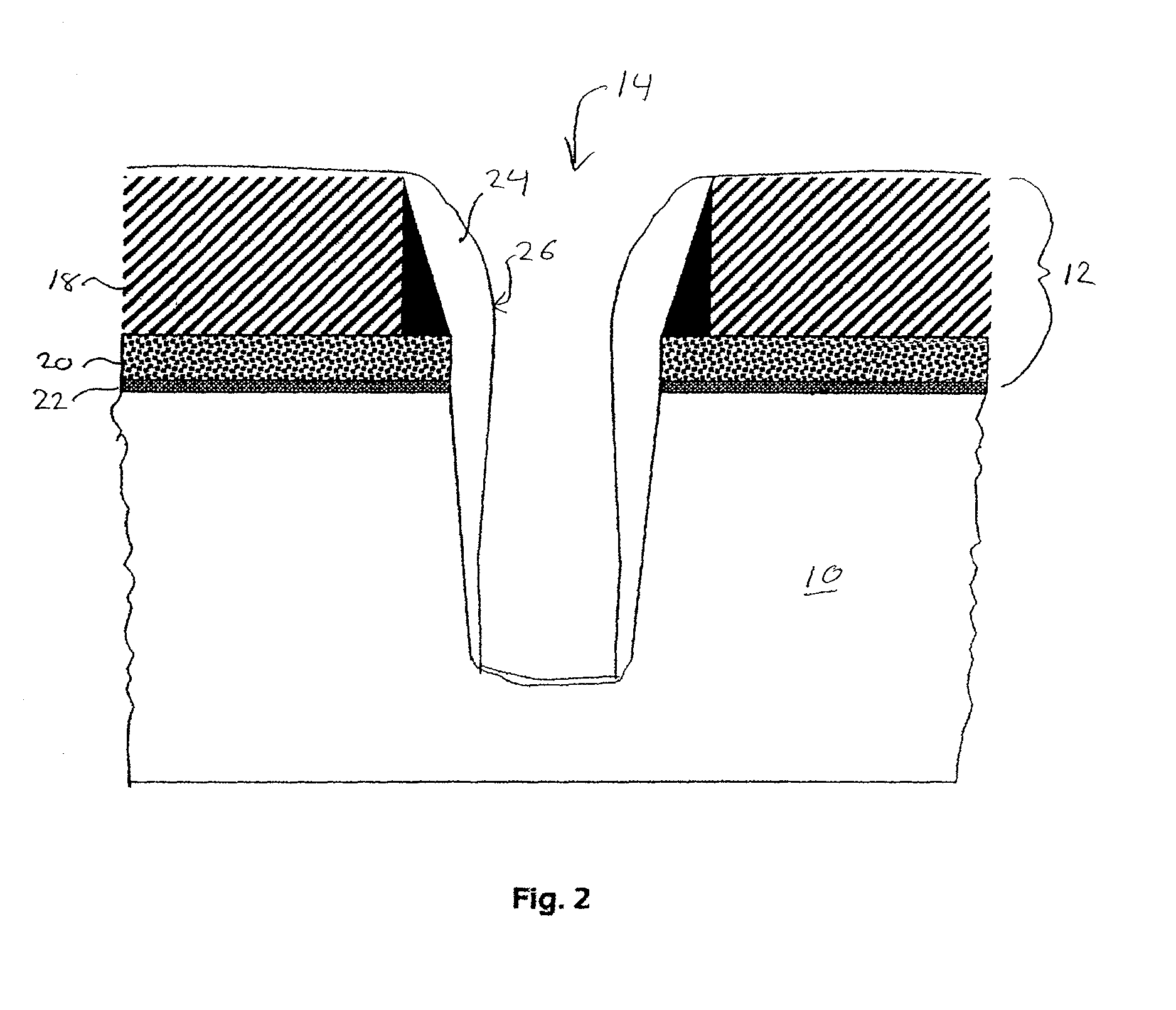
[0031] In describing the preferred embodiment of the present invention, reference will be made herein to FIGS. 1-4 of the drawings in which like numerals refer to like features of the invention. Features of the invention are not necessarily shown to scale in the drawings.

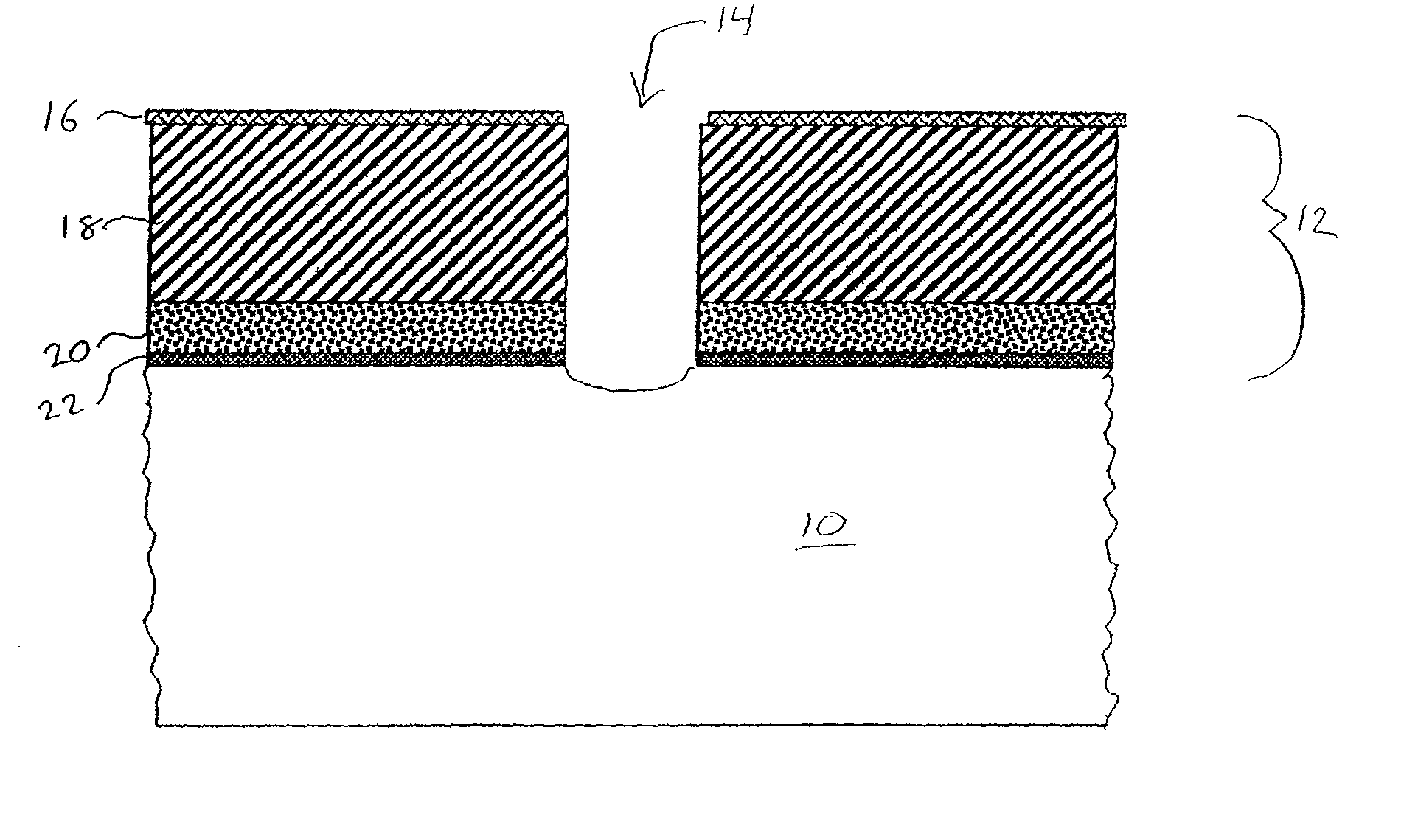
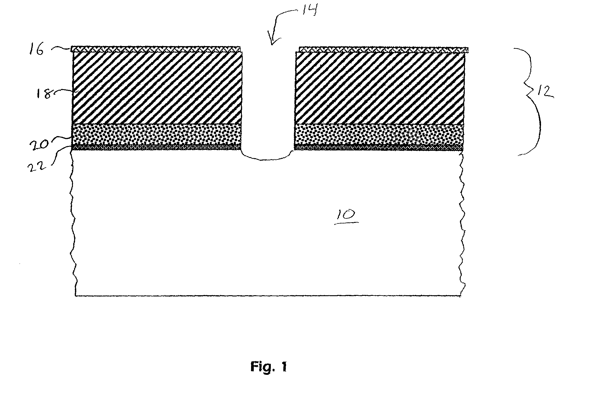
[0032] FIG. 1 shows a wafer having a substrate 10 and a patterned hard mask stack 12 on the upper surface of the substrate 10. The hard mask stack includes an opening 14 that defines the width of a high aspect ratio opening to be produced in the substrate 10 by the method of this invention.

[0033] Opening 14 is produced in the hard mask stack 12 in a conventional manner and FIG. 1 illustrates the wafer without the resist material used to create opening 14. The wafer in FIG. 1 is shown substantially as it appears prior to being inserted into a plasma reactor for reactive ion etching using the method of this invention.

[0034] The hard mask stack 12 includes a cap oxide layer 16. The cap oxide layer 16 is preferably a p...


PUM

PropertyMeasurementUnit
widthaaaaaaaaaa
pressureaaaaaaaaaa
temperatureaaaaaaaaaa

Abstract

A method of etching a deep, high aspect ratio opening in a silicon substrate includes etching the substrate with a first plasma formed using a first gaseous mixture including a bromine containing gas, an oxygen containing gas and a first fluorine containing gas. The etching process with the first gaseous mixture produces a sidewall passivating deposit, which builds up near the opening entrance. To reduce this buildup, and to increase the average etching rate, the sidewall passivating deposit is periodically thinned by forming a second plasma using a mixture containing silane and a second fluorine containing gas. The substrate remains in the same plasma reactor chamber during the entire process and the plasma is continuously maintained during the thinning step. Holes of a depth greater than 40 times the width may be produced using repeated cycles of etching and thinning.

Description

[0001] 1. Field of the Invention[0002] This invention relates to etching deep, high aspect ratio openings in a substrate during the construction of microelectronic devices. More specifically, this invention relates to etching such openings using a reactive ion etching process in plasma reactor.[0003] 2. Description of Related Art[0004] The fabrication of deep, high aspect ratio openings and trenches in a silicon substrate is desirable in several areas of ultra large scale integration (ULSI) processing. Trenches having a depth:width ratio of greater than about 15:1 may be considered high aspect ratio, but trenches having an aspect ratio of greater than 40:1 are occasionally required.[0005] Plasma reactors are conventionally used to construct high aspect ratio openings using a reactive ion etching (RIE) process in which one or more gaseous etchants are used to simultaneously etch the opening and produce a sidewall passivating deposit during the etching process. The sidewall passivatin...

Claims


Application Information

Patent Timeline
Patent Type & Authority Applications(United States)
IPC IPC(8): B44C1/22C03C25/68C23F1/00H01L21/00H01L21/302H01L21/3065H01L21/308H01L21/762
CPCH01L21/3065H01L21/76224H01L21/3081H01L21/30655
Inventor MATHAD, GANGADHARA S.PANDA, SIDDHARTHARANADE, RAJIV M.
Owner INFINEON TECH AG
Why Eureka
Try Eureka