

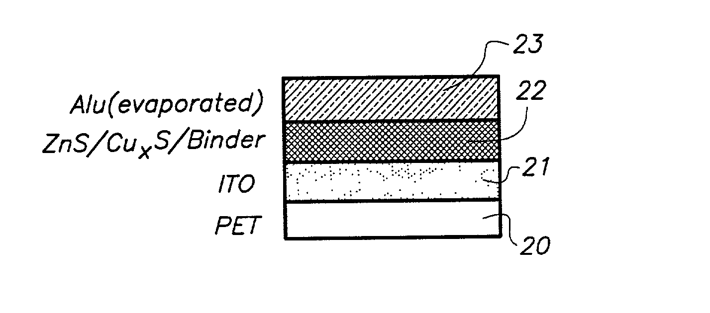
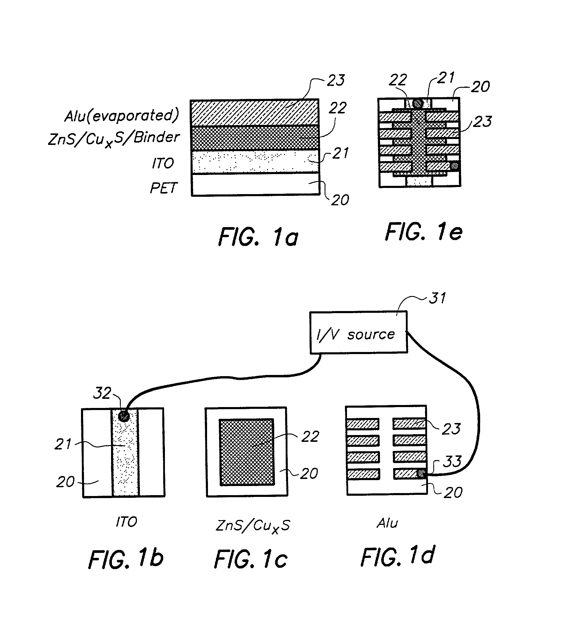
Manufacturing of a thin film inorganic light emitting diode
a technology of inorganic light and diodes, which is applied in the direction of zinc sulfide, chemistry apparatus and processes, and light-emitting compositions. it can solve the problems of low fluorescent quantum yield, cumbersome and expensive vacuum-vapour deposition techniques, and low fluorescent quantum yield of tfel devices, and achieves easy and economical
- Summary
- Abstract
- Description
- Claims
- Application Information
AI Technical Summary
Benefits of technology
Problems solved by technology
Method used
Image

Examples
Embodiment Construction
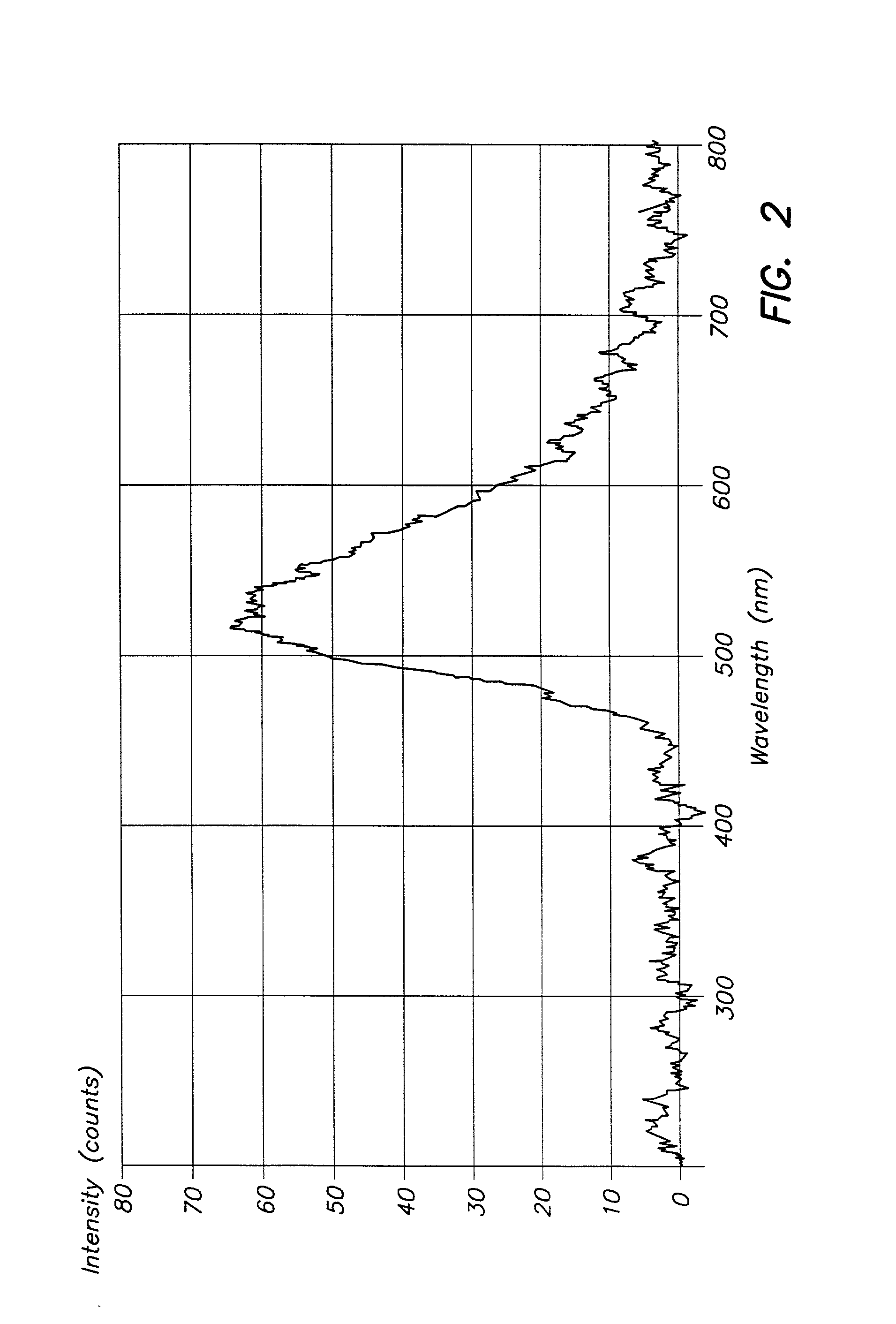
1. Green Emitting Single Layer ILEDs
[0075] 1.1. Preparation of the Zn(Cu(1%))S--Dispersion:
[0076] The following solutions were prepared:
1 Solution 1 ZnCl.sub.2.2H.sub.2O 81.76 g Water to 600 ml Solution 2 Na.sub.2S.9H.sub.2O 141.6 g NaOH (50%) 3.6 ml Water to 600 ml Solution 3 CuCl.sub.2 0.85 g Water to 800 ml
[0077] The ZnS:Cu dispersion was prepared as follows:
[0078] To solution 3, stirred at 1500 rpm at room temperature, was firstly added 0.5 ml of solution 2. Subsequently, solutions 1 and 2, both held at room temperature, were added simultaneously at a flow rate of 500 ml / min to solution 3. This is the predispersion A comprising ZnS:Cu--particles.
[0079] 1.2. Washing of the Zn(Cu)S--Dispersion:
[0080] To 1000 ml of predispersion A, 1000 ml of a 2% Na-polyphosphate solution in water was added and this dispersion was diafiltrated through a Fresenius F60 cartridge. The dispersion was concentrated to 1000 ml and washed at this level by using 6000 ml of a 2% solution of Na-polyphosphate...
PUM
| Property | Measurement | Unit |
|---|---|---|
| thick | aaaaa | aaaaa |
| thick | aaaaa | aaaaa |
| thick | aaaaa | aaaaa |
Abstract
Description
Claims
Application Information