Source voltage conversion circuit and its control method, display, and portable terminal

a conversion circuit and source voltage technology, applied in the direction of efficient power electronics conversion, static indicating devices, instruments, etc., can solve the problems of insufficient driving voltage for switching transistors, increase in circuit area, decrease in current capacity, etc., to achieve stable dc-to-dc conversion operation, improve conversion efficiency, and high current capacity

Active Publication Date: 2003-01-16
JAPAN DISPLAY INC
View PDF4 Cites 42 Cited by
  • Summary
  • Abstract
  • Description
  • Claims
  • Application Information

AI Technical Summary

Benefits of technology

0077] Thus, since a sufficient switching current is obtained in the Pch MOS transistor Qp12, it is possible to perform stable DC-to-DC conversion operation and improve conversion efficiency. In particular, since a sufficient switching current is obtained without increasing transistor size of the Pch MOS transistor Qp12, it is possible to realize a DD converter having a high current capacity on a small-area circuit scale. Its effect is especially great when a transistor with a high threshold value Vth, for example a thin film transistor is used.

Problems solved by technology

Therefore, a sufficient driving voltage may not be provided for the switching transistors, particularly the Pch MOS transistor Qp102.
The increase in the transistor size results in a problem such as an increase in circuit area or a decrease in current capacity.
This results in a problem such as a decrease in current capacity.
The above problem becomes serious both when a threshold value Vth of the transistor is great and when variation in the threshold value Vth is great.
It is known that amorphous silicon and polysilicon used to form the thin film transistors have inferior crystallinity and inferior controllability of the conducting mechanism to single-crystal silicon, and thus the formed thin film transistors have great variations in characteristics.

Method used


Image

  • Source voltage conversion circuit and its control method, display, and portable terminal
  • Source voltage conversion circuit and its control method, display, and portable terminal
  • Source voltage conversion circuit and its control method, display, and portable terminal

Examples


second application example

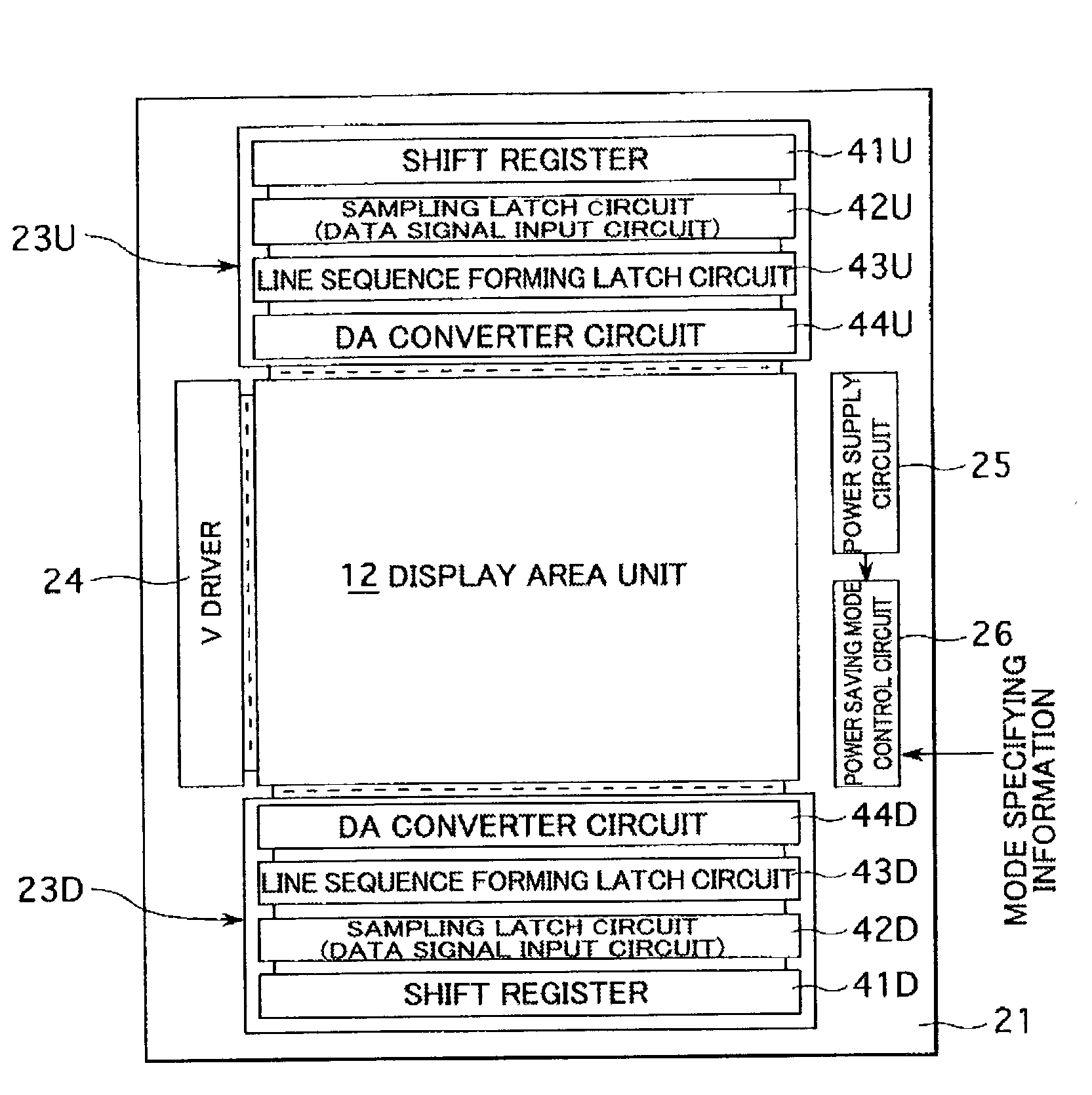
[0148] Provided in view of the above is a display apparatus, for example an active matrix type liquid crystal display apparatus according to a second application example to be described below. FIG. 33 is a schematic block diagram showing an example of configuration of the active matrix type liquid crystal display apparatus according to the second application example of the present invention. In the figure, the same parts as in FIG. 15 are identified by the same reference numerals.

[0149] The active matrix type liquid crystal display apparatus according to the second application example is configured such that a synchronizing signal, for example a horizontal synchronizing signal HD in synchronism with a video signal displayed on a display area unit 12 is used as a switching pulse of a power supply circuit 25 formed by a charge pump type DD converter, and such that a timing control circuit 28 is integrated on the same glass substrate 21 of the display area unit 22. The other configurat...


PUM


Abstract

In a power supply voltage converting circuit using a charge pump circuit having a switch device (Nch MOS transistor Qn(12) and Pch MOS transistor Qp(12)) in an output unit, a first clamp circuit (13) diode-clamps a switching pulse voltage (control pulse voltage) for the switch device at the time of starting the power supply voltage converting circuit, and a second clamp circuit (16) clamps the switching pulse voltage at a ground level (negative side circuit power supply potential) on the basis of a clamp pulse obtained by using an output voltage Vout at the time of an end of the starting process. A sufficient driving voltage is thereby provided for the Pch MOS transistor Qp(12) in particular. Thus, a power supply voltage converting circuit that can obtain a high current capacity on a small-area circuit scale, a control method thereof, a display apparatus having the power supply voltage converting circuit as a power supply circuit, and a portable terminal having the display apparatus are provided.

Description

[0001] The present invention relates to a power supply voltage converting circuit, a control method thereof, a display apparatus, and a portable terminal, and particularly to a power supply voltage converting circuit using a charge pump circuit, a control method thereof, a display apparatus having the power supply voltage converting circuit as a power supply circuit, and a portable terminal having the display apparatus.[0002] Portable terminals such as portable telephones and PDAs (Personal Digital Assistants) have recently spread remarkably. One of factors in the rapid spread of these portable terminals is a liquid crystal display apparatus mounted as an output display unit of the portable terminals. The reason is that in principle, the liquid crystal display apparatus has a characteristic of not requiring much power for driving the liquid crystal display apparatus and is therefore a display device of low power consumption.[0003] A portable terminal uses a single power supply volta...

Claims


Application Information

Patent Timeline
Patent Type & Authority Applications(United States)
IPC IPC(8): G09G3/36H02M3/07
CPCG09G3/3696G09G2330/02H02M3/07H02M2001/0012H02M2001/0032Y02B70/16G09G2320/0233G09G2300/0408G09G2310/04G09G2330/022G09G2340/0428Y02B70/10H02M1/0012H02M1/0032H02M3/071
Inventor NAKAJIMA, YOSHIHARU
Owner JAPAN DISPLAY INC
Why Eureka
Try Eureka