Surface emitting semiconductor laser

Inactive Publication Date: 2003-02-27
FUJIFILM BUSINESS INNOVATION CORP
View PDF0 Cites 56 Cited by
  • Summary
  • Abstract
  • Description
  • Claims
  • Application Information

AI Technical Summary

Problems solved by technology

For example, manufacturing costs of the VCSEL are low, productivity is high, and achieving a two-dimensional array is easy, coupling efficiency with an optical fiber is high, and electric power consumption is low.
However, fundamental lateral made optical output power of conventional VCSELs remains small, or roughly 1 mW at most.
Therefore, the application range of conventional VCSELs has been limited to narrow fields, such as a light pick-up used in a CD-ROM drive.
With conventional VCSELs, because laser oscillation by the fundamental lateral mode has been obtained by narrowing the diameter of an optical emission region to roughly several .mu.m, the volume of an active region has been resultantly small, and fundamental lateral mode optical output power has been low.
However, at the same time, there are also problems in that a negative influence is exerted on fundamental lateral mode characteristics, and it is considerably difficult to stably form the loss determination element 176 of a predetermined configuration.
As Kenichi Iga and Fumio Koyama describe in "Surface emitting Laser" (Ohm, 1990), because it is difficult for the surface emitting semiconductor laser to earn gains necessary for the laser oscillation due to the active region being small, generally a high reflectance is necessary for the cavity.
As a result, it is surmised that a sufficient high-intensive fundamental lateral mode optical output power will become unobtainable.
However, even based on present etching technologies, it is substantially difficult to form with good reproducibility and without positional dependency a curved surface at always the same position.
This problem becomes particularly pronounced when a large number of VCSEL elements is provided to form a two-dimensional array.
Moreover, it is extremely difficult to finish the etching at a proper position either at the point the layer 184 working as the etching mask in the RIE process disappears or thereafter, in order to form the loss determination element 176 having a predetermined, curved-surface configuration and a predetermined film thickness.
In addition, when a large number of VCSEL elements is provided to form a two-dimensional array, it is extremely difficult to control with high precision an etching selection ratio between materials that structure the photoresist pillar 183 and the loss determination element 176 on the same substrate or on different substrates.
Therefore, it is extremely difficult to match reflectance characteristics of the loss determination element 176 between each of the VCSEL elements.
As described above, it is extremely difficult to eliminate or minimize variations in the shape and film thickness of the loss determination elements 176 between VCSEL elements on the same substrate, between VCSEL elements on different substrates, or between VCSEL elements in which lots in processes are different.
Therefore, it is difficult to industrially utilize for purposes in which a high-intensity fundamental lateral mode op

Method used


Image

  • Surface emitting semiconductor laser
  • Surface emitting semiconductor laser
  • Surface emitting semiconductor laser

Examples


first embodiment

[0107] First Embodiment

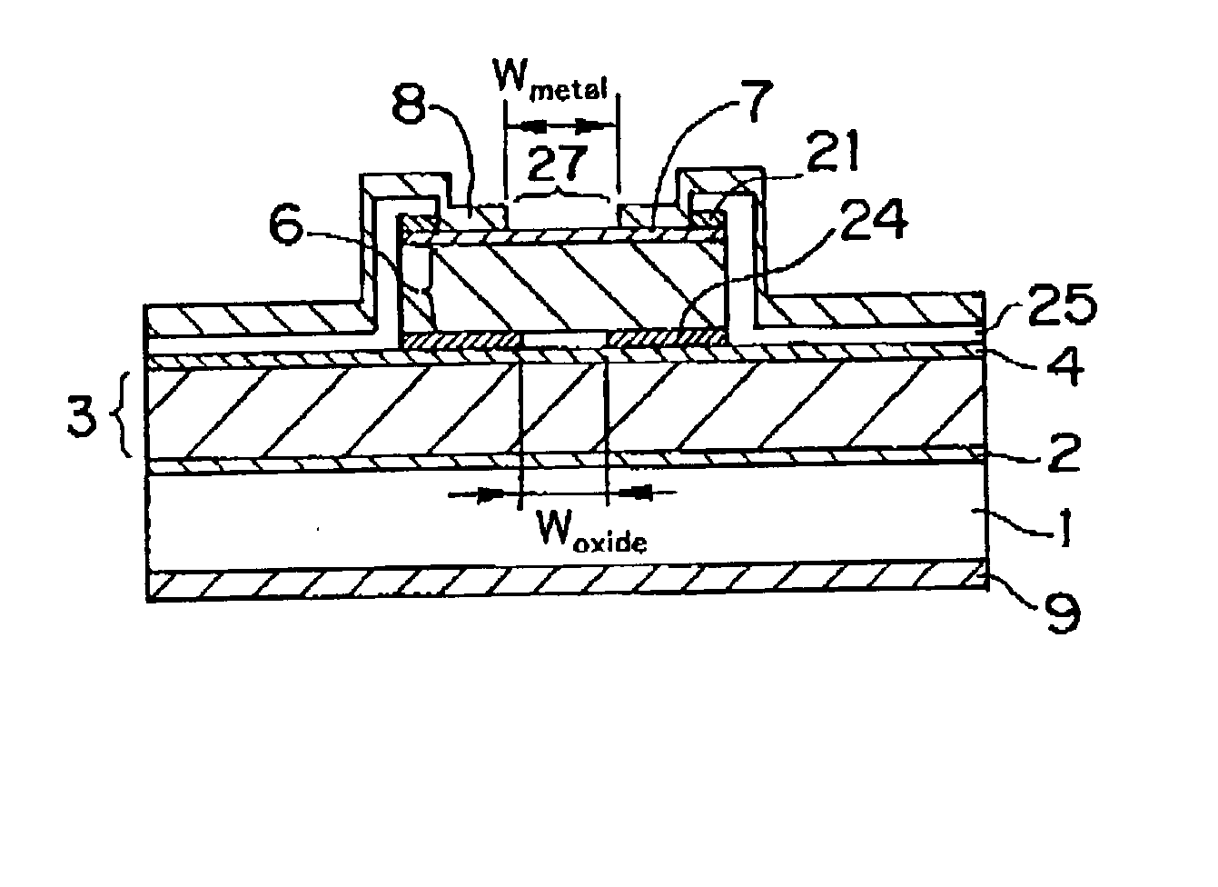
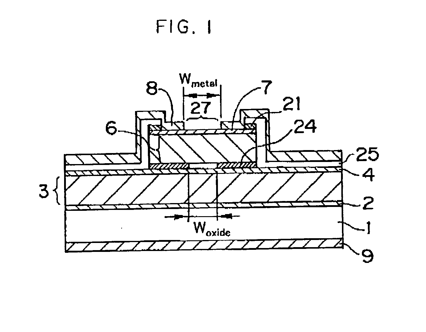
[0108] A structure of a VCSEL relating to a first embodiment of the present invention will be explained with reference to FIGS. 5A to 5G that illustrate a manufacturing process of the VCSEL.

[0109] As illustrated in FIG. 5A, using a metal organic chemical vapor deposition (MOCVD) method, an n-type GaAs buffer layer 2, a lower n-type DBR layer 3, an active region 4, a p-type AlAs layer 5, an upper p-type DBR layer 6, and a p-type GaAs contact layer 7 are sequentially layered on an n-type GaAs substrate 1.

[0110] The n-type GaAs buffer layer 2 has a film thickness of 0.2 .mu.m, and is composed of n-GaAs having a carrier density of 1.times.10.sup.18 cm.sup.-3 after doping Si as an n-type impurity. The n-type GaAs buffer layer 2 fulfills a role of smoothly advancing an epitaxial growth including Al thereafter.

[0111] The lower n-type DBR layer 3 is a plural-layer layered product having alternately layered by 40.5 cycles n-type Al.sub.0.9 Ga.sub.0.1As and n-type Al.su...

second embodiment

[0126] Second Embodiment

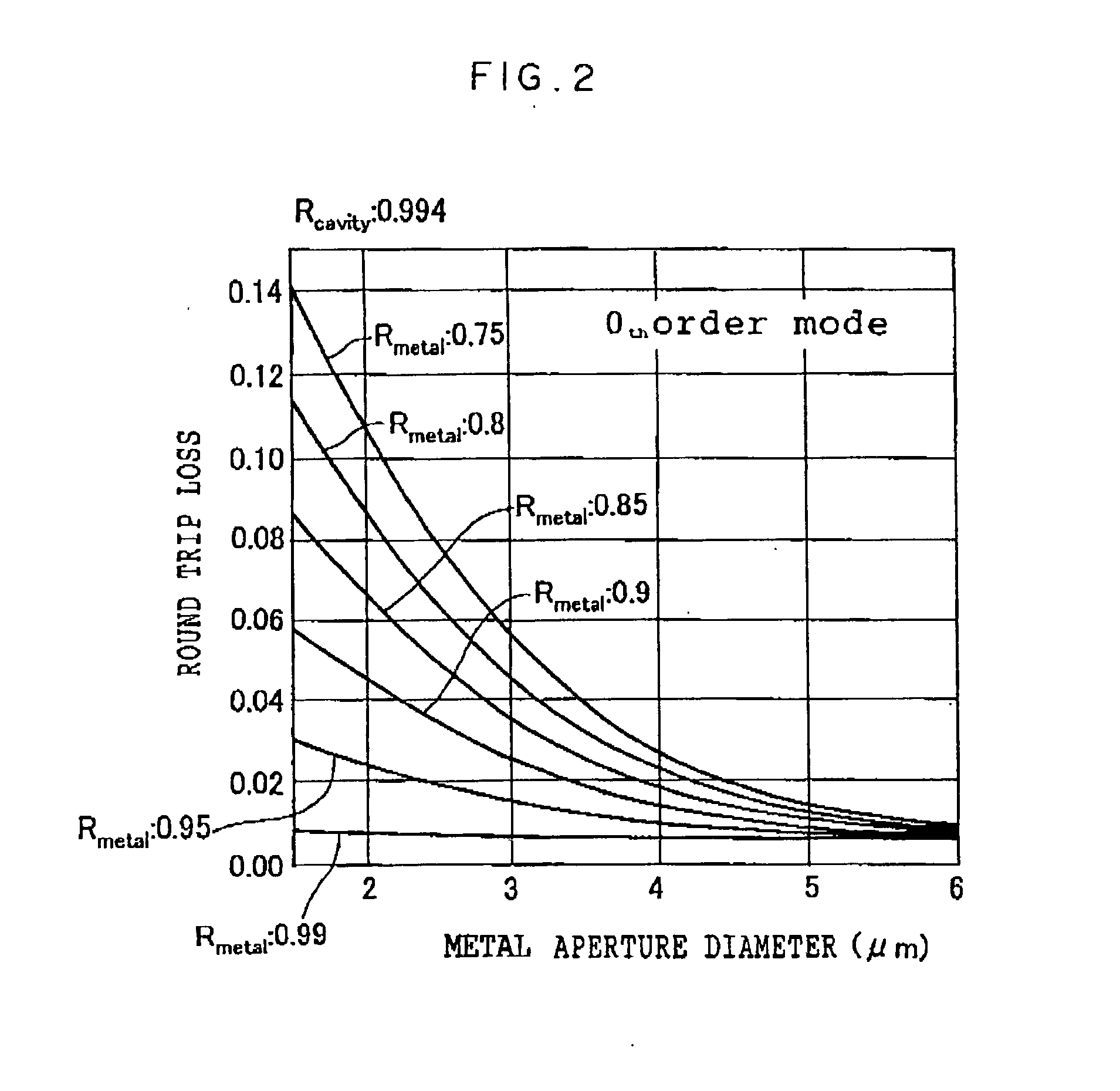
[0127] A VSCEL relating to a second embodiment of the present invention will be explained next. In the first embodiment, a description has been made of the behavior of the fundamental lateral mode optical output power when the metal aperture diameter is changed by assuming that the aperture diameter of the current confinement portion is 3.5 .mu.m. In the second embodiment, the dependency of the fundamental lateral mode optical output power on the metal aperture diameter when the aperture diameter of the current confinement portion is changed will be explained. The structure of the laser itself remains unchanged from that of the first embodiment and therefore, the explanation of the laser will be omitted here. Elements having the aperture diameter of the current confinement portion as 3 .mu.m, 4 .mu.m and 5 .mu.m are manufactured by adjusting the heat treatment time for selectively oxidizing the AlAs layer 5.

[0128] FIG. 8 shows a result of an electrooptic eval...

third embodiment

[0135] Third Embodiment

[0136] A VCSEL pertaining to a third embodiment of the present invention will be described. In the first and second embodiments, examples have been given in which, by using two kinds of electrode materials. Ti and Au, administering an EB deposition at a film thickness of 10 nm for Ti and 30 nm for Au, and thereafter performing a heat treatment at an environmental temperature of 350.degree. C. for ten minutes, the upper electrode is formed and the reflectance of the cavity of the region corresponding to the upper electrode is lowered. With the exception of conditions for forming the upper electrode, the present embodiment is similar to the first embodiment, and because the structure of the laser itself is the same as that described in this first and second embodiments, description thereof will be omitted.

[0137] Methods for lowering the reflectance of a cavity by providing the upper electrode include, for example, the following two methods.

[0138] (1) A method in...


PUM


Abstract

The present invention provides a surface emitting semiconductor laser, comprising: a semiconductor substrate having sequentially layered thereon a lower multi-layer mirror, an active layer region, and an upper multi-layer mirror that, together with the lower multi-layer mirror, contributes to the formation of a cavity; an upper electrode disposed on an upper layer of the upper multi-layer mirror and provided with an aperture that forms an emission region of a laser beam generated at the active layer region; and a current confinement portion disposed between the upper electrode and the lower multi-layer mirror and provided with an aperture that forms a current path; wherein an aperture diameter of the upper electrode and an aperture diameter of the current confinement portion are determined such that a difference between an optical loss of the cavity in a higher-order lateral mode of the laser beam and an optical loss of the cavity in a fundamental lateral mode of the laser beam becomes a value in the vicinity of a maximum value, and the higher-order lateral mode is suppressed, and at least one of the aperture formed in the upper electrode and the aperture of the current confinement portion is formed into a two-fold symmetrical configuration having long and short axes with respect to arbitrary two axial directions orthogonal to each other in a plane.

Description

[0001] 1. Field of the Invention[0002] The present invention relates to a surface emitting semiconductor laser, and more particularly to a surface emitting semiconductor laser with which oscillation of high-output, fundamental lateral mode light is possible.[0003] The present invention further relates to a surface emitting semiconductor laser. More particularly, the present invention relates to a surface emitting semiconductor laser which can oscillate high-output fundamental lateral mode light, and a structure of an element in which polarization of light is controlled and which has high utility value as a light source employed for optical information processing or optical communication or a light source for a xerographic image forming apparatus.[0004] 2. Description of Related Art[0005] In comparison with an edge emitting laser, a vertical cavity surface emitting laser (hereinafter referred to as "VCSEL") has numerous merits. For example, manufacturing costs of the VCSEL are low, p...

Claims


Application Information

Patent Timeline
IPC IPC(8): H01S5/183
CPCH01S5/0421H01S5/0425H01S5/18311H01S5/18338H01S5/18388H01S5/18394H01S2301/166H01S2301/18H01S5/04254H01S5/18333H01S5/04252
Inventor UEKI, NOBUAKISAKAMOTO, AKIRAYOSHIKAWA, MASAHIRONAKAYAMA, HIDEOOTOMA, HIROMI
Owner FUJIFILM BUSINESS INNOVATION CORP
Why Eureka
Try Eureka