Partially removable spacer with salicide formation

a technology of partially removable spacers and transistors, applied in the direction of basic electric elements, electrical apparatus, semiconductor devices, etc., can solve the problems of reducing device performance, reducing device selectivity, and obsolete or otherwise unacceptable known processing steps,

Inactive Publication Date: 2003-03-06
IBM CORP
View PDF0 Cites 4 Cited by
  • Summary
  • Abstract
  • Description
  • Claims
  • Application Information

AI Technical Summary

Benefits of technology

[0010] It is another object of the invention to provide a field effect transistor structure of extremely small size in which performance is not compromised by the manufacturing process.
[0011] In order to accomplish these and other objects of the invention, a method for fabrication of a semiconductor device and a semiconductor device formed by the method are provided wherein the fabrication process includes the steps of forming a composite sidewall on lateral sides of a polysilicon gate structure on a dielectric layer on a substrate, performing self-aligned silicidation on the polysilicon gate structure and portions of the substrate exposed by patterning of the dielectric layer, partially removing the composite sidewall to expose a further area of the substrate, and implanting impurities in the further area of said substrate. This method allows implantation of the impurities to be performed subsequent to the metal deposition and annealing of the silicidation operation and thus maintained at a shallow depth for high performance of the device.

Problems solved by technology

However, the small size of device structures possible at the current state of the art occasionally make known processing steps obsolete or otherwise unacceptable.
The salicide annealing process can deactivate impurities and cause additional movement or diffusion of the dopant or impurity which may diminish device performance if performed subsequent to the source / drain implant and annealing processes.
However, while the selectivity of the salicidation process (i.e. the process proceeds on all exposed silicon surfaces but not on insulators such as silicon nitride and silicon oxide) is generally exploited in semiconductor device construction, the very selectivity of the process does not allow salicidation to precede the implantation process.
That is, the implantation process must be done on a bare silicon surface to be adequately controllable and present processes have not provided a practical approach to avoiding salicidation of the locations where the implant is to be performed, when left bare.
Further, since salicide or silicide is highly conductive, bridging between the source and / or drain and the gate must be avoided which, at the present state of the art, cannot be achieved if insulative spacers are not present on the gate sidewalls.
However, in practice, the removal of the second sidewall layer would also remove isolation oxide which is formed between transistors (as well as other structures such as capacitors) and elevate perimeter leakage due to the silicide wrap-around.
Accordingly, it is seen that there is a conflict between a process employing implantation before salicidation which is likely to compromise device performance by the annealing associated with salicidation and a process employing salicidation before implantation which cannot, at the present state of the art, reliably provide an operative device structure, much less a satisfactory manufacturing yield.

Method used


Image

  • Partially removable spacer with salicide formation
  • Partially removable spacer with salicide formation
  • Partially removable spacer with salicide formation

Examples


Embodiment Construction

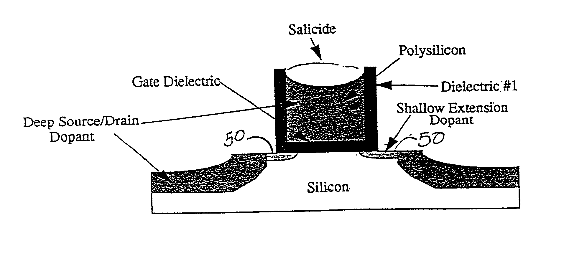
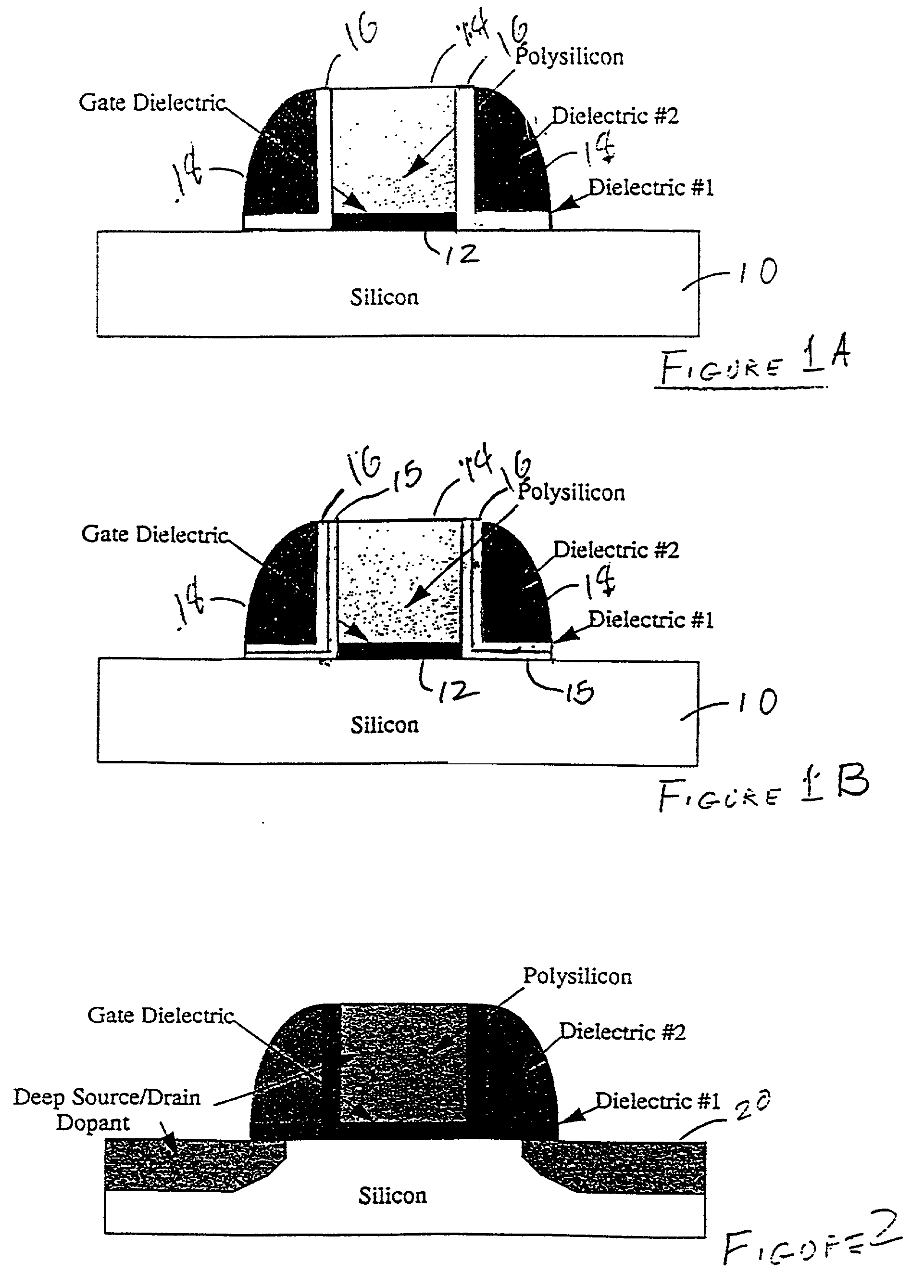
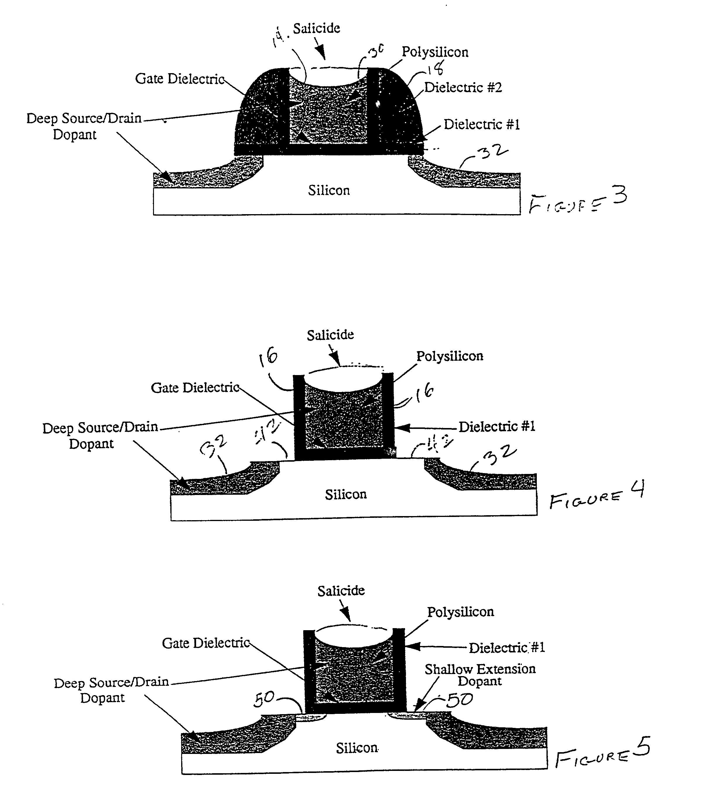
[0018] Referring now to the drawings, and more particularly to FIG. 1, there is shown, in cross-sectional form, an early stage in the fabrication of the invention. It is to be understood that none of the Figures are to scale or proportioned to reflect any particular transistor design and that some features not important to the practice of the invention or which are conventional are omitted in the interest of clarity. It is also to be understood that the salient features of the invention are depicted in FIGS. 1-5 in a manner to facilitate an understanding of the principles of the invention by those skilled in the art and in the general form preferred by the inventors at the present time. However, as will be understood by those skilled in the art in view of the following description of the invention, the principles of the invention can be practiced in numerous other forms than that depicted.

[0019] To achieve the state shown in FIG. 1, a gate dielectric 12 is first deposited or grown o...


PUM

PropertyMeasurementUnit
densityaaaaaaaaaa
sizeaaaaaaaaaa
integration densityaaaaaaaaaa

Abstract

Formation of sidewalls on a gate structure in layers having a differential etch rate for certain etchants allows metallization and salicide formation annealing of a gate electrode and source / drain regions prior to shallow impurity implantation and impurity activation annealing at the location of a removable portion of a sidewall spacer establishing a gap between source / drain regions and remaining sidewalls of a gate structure. Therefore, diffusion of impurities to a greater depth and impurity deactivation during salacide formation annealing is avoided in a high performance semiconductor device such as a field effect transistor of extremely small dimensions.

Description

[0001] 1. Field of the Invention[0002] The present invention generally relates to advanced field effect transistors and, more particularly, to manufacturing processes for manufacturing high-performance field effect transistors at extremely small size.[0003] 2. Description of the Prior Art[0004] Field effect transistors (FETs), at the present state of the art, are the integrated circuit active switching element of choice for all but the most critical of high density integrated circuit designs. As is recognized in the art, high integration density and extremely small device size provides benefits of improved performance and increased chip functionality as well as manufacturing economies. Small device size and high density provide short signal propagation paths, increasing operational speed while providing more switching devices and circuits on a single chip that can be manufactured by a given set of process steps. At the present state of the art, so-called self-aligned processes are k...

Claims


Application Information

Patent Timeline
Patent Type & Authority Applications(United States)
IPC IPC(8): H01L21/336
CPCH01L29/66492H01L29/665H01L29/6653
Inventor AGNELLO, PAUL D.CROWDER, SCOTT W.SMEYS, PETER
Owner IBM CORP
Why Eureka
Try Eureka