Bi-layer silicon film and method of fabrication

a technology of silicon film and bilayer, applied in the direction of coating, transistor, chemical vapor deposition coating, etc., can solve the problem of affecting the performance of the fabricated transistor in a negative way

Inactive Publication Date: 2003-03-13
APPLIED MATERIALS INC
View PDF6 Cites 56 Cited by
  • Summary
  • Abstract
  • Description
  • Claims
  • Application Information

AI Technical Summary

Benefits of technology

[0017] The perpendicular grain boundaries 110 provide a path for the fast defusion of dopants, such as boron, during subsequent ion-implantation and thermal anneal steps. The random grains 106 and therefore grain boundaries 114 of the lower polycrystalline silicon film greatly reduces or slows down dopant diffusion within the film. The lower polycrystalline silicon film 102 can therefore be used to prevent dopant diffusion into underlying films, such as gate oxides. By forming a bi-layer silicon film 100 with a top columnar structure the composite film 100 is characterized as having a fast diffusion within the columnar portion of the film and a diffusion barrier in the lower portion of the film. The thickness of the lower polycrystalline silicon film 102 is kept as thin as possible but yet is thick enough to prevent dopants from diffusing therethrough while the film is heated to a temperature and for a period of time necessary to activate the incorporated dopant. In order to provide good blocking functionality lower polycrystalline silicon film 104 should be at least several grains thick. Additionally, the thickness of the upper columnar grain silicon film 104 is kept sufficiently thick to control the resistivity of the fabricated electrode. In an embodiment of the present invention, the lower polycrystalline silicon film 102 has a thickness between 200-500 .ANG. and the upper polycrystalline silicon film 104 has a thickness between 1200-1800 .ANG. for a total thickness of the bi-layer silicon film 100 of approximately 1500-2000 .ANG..

Problems solved by technology

The lack of uniform distribution of dopants in the polysilicon, known as "poly depletion", detrimentally affects the performance of the fabricated transistor especially as a gate lengths decrease to below 0.18 microns.

Method used


Image

  • Bi-layer silicon film and method of fabrication
  • Bi-layer silicon film and method of fabrication
  • Bi-layer silicon film and method of fabrication

Examples


Embodiment Construction

[0014] The present invention is a novel bi-layer silicon film and its method of fabrication. In the following description, for purposes of explanation, numerous specific details are set forth in order to provide a thorough understanding of the present invention. It will be evident, however, to one skilled in the art that the present invention may be practiced without these specific details. In other instances, specific apparatus structures and methods have not been described so as not to obscure the present invention.

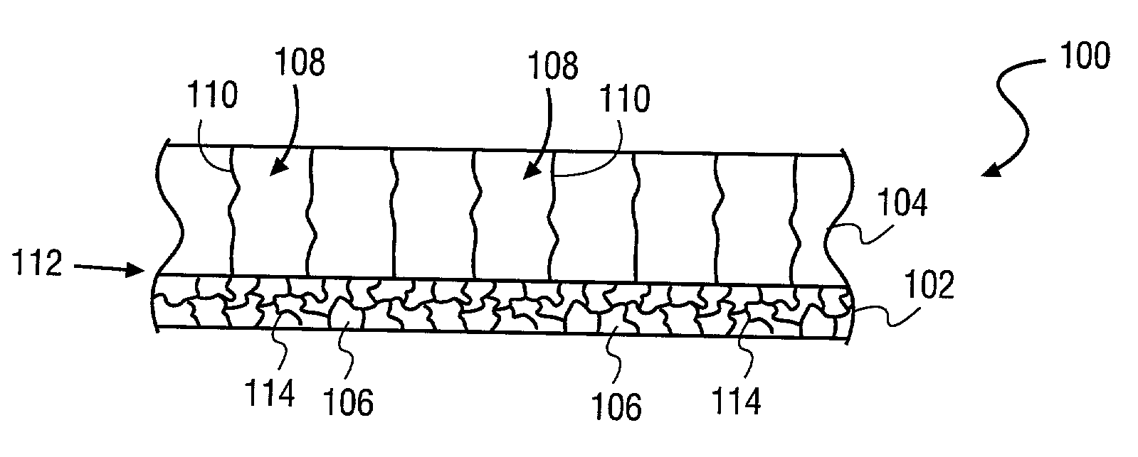
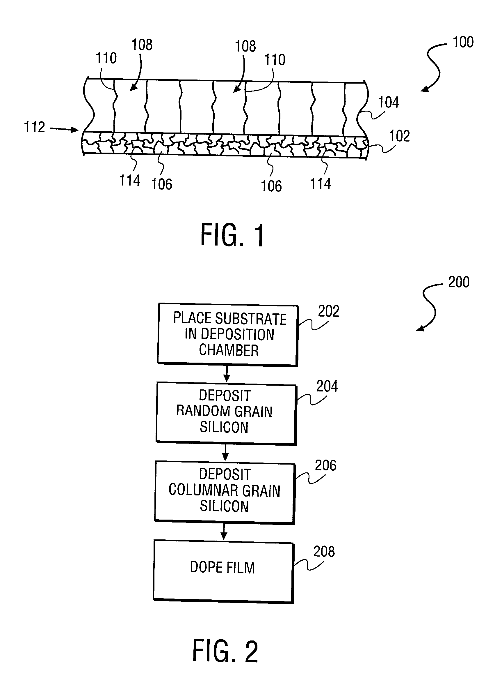
[0015] The present invention is a novel bi-layer silicon film and its method of fabrication. An example of a bi-layer silicon film 100 in accordance with the present invention is illustrated in FIG. 1. Bi-layer silicon film 100 includes an upper polycrystalline silicon film 104 formed directly on a lower polycrystalline silicon film 102. Lower polycrystalline silicon film 102 is a polycrystalline silicon film having small and random grain boundary structure as opposed t...


PUM

PropertyMeasurementUnit
temperatureaaaaaaaaaa
thicknessaaaaaaaaaa
thicknessaaaaaaaaaa

Abstract

A bi-layer silicon electrode and its method of fabrication is described. The electrode of the present invention comprises a lower polysilicon film having a random grain microstructure, and an upper polysilicon film having a columnar grain microstructure.

Description

[0001] 1. FIELD OF THE INVENTION[0002] The present invention relates to the field of semiconductor integrated circuit manufacturing and more specifically to a bi-layer silicon film and its method of fabrication.[0003] 2. DISCUSSION OF RELATED ART[0004] In order to fabricate more complex and higher density integrated circuits such as microprocessors and memories, the size of device features must be continually reduced. An important feature which must be reduced in order to increase device density is the polysilicon gate length and correspondingly the polysilicon thickness of MOS transistors. Present polysilicon deposition processes form polysilicon films 802 having large and columnar grains 804 as shown in FIG. 6. The large and columnar grains 804 are beginning to play a critical role in the performance of the transistor as transistor gate lengths are shrunk to less than 0.18 microns. Dopants 806 which are subsequently added to the polysilicon film in order to reduce the resistance o...

Claims


Application Information

Patent Timeline
Patent Type & Authority Applications(United States)
IPC IPC(8): H01L21/28H01L29/49
CPCH01L21/28035H01L29/4925Y10S438/969
Inventor FU, LIWANG, SHULINLEE, LUOCHEN, STEVEN A.SANCHEZ, ERROL
Owner APPLIED MATERIALS INC
Why Eureka
Try Eureka