Multi-stage, high frequency, high power signal amplifier

a signal amplifier and high-frequency technology, applied in the field of high-frequency, can solve the problems of limited ability to successfully tune transistor devices on a large-scale manufacturing basis, large-scale manufacturing of power transistor devices and amplifiers in high-frequency applications, and difficult large-scale manufacturing. achieve the effect of uniform performance and easy large-scale manufacturing

Inactive Publication Date: 2003-04-24
INFINEON TECH AG
View PDF0 Cites 20 Cited by
  • Summary
  • Abstract
  • Description
  • Claims
  • Application Information

AI Technical Summary

Benefits of technology

0005] In accordance with a general aspect, inventions disclosed and described herein are directed to high frequency, high power (hereinafter "broadband") RF

Problems solved by technology

Production of RF power transistors on a large-volume basis is traditionally problematic, because of natural variables that the individual transistor elements possess.
Due to the variations in transistors' and various other elements over identical operating frequencies and voltages, however, the ability to successfully tune transistor devices on a large scale manufacturing basis is limited.
Such problems with large scale manufacturing of power transi

Method used


Image

  • Multi-stage, high frequency, high power signal amplifier
  • Multi-stage, high frequency, high power signal amplifier
  • Multi-stage, high frequency, high power signal amplifier

Examples


Embodiment Construction

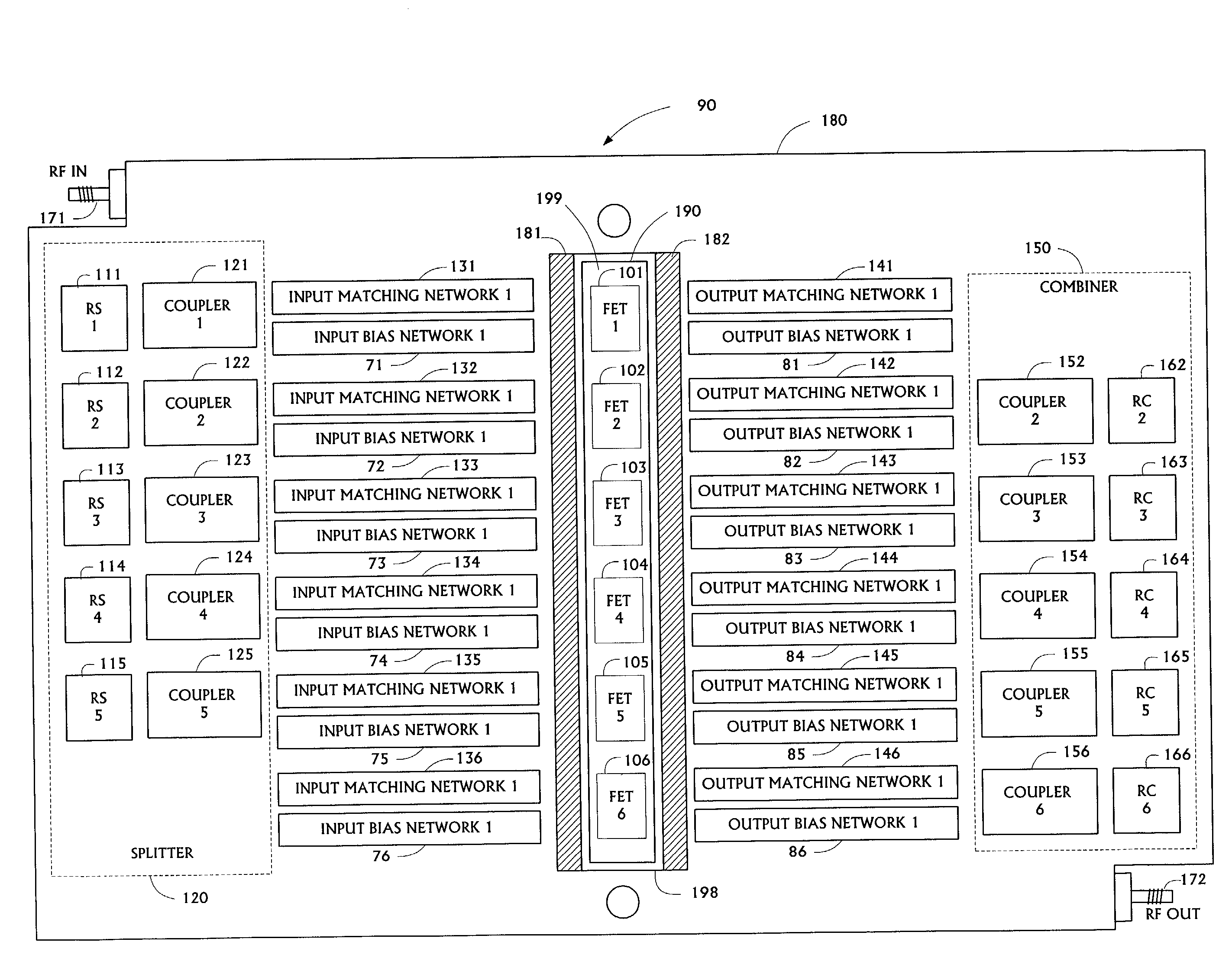
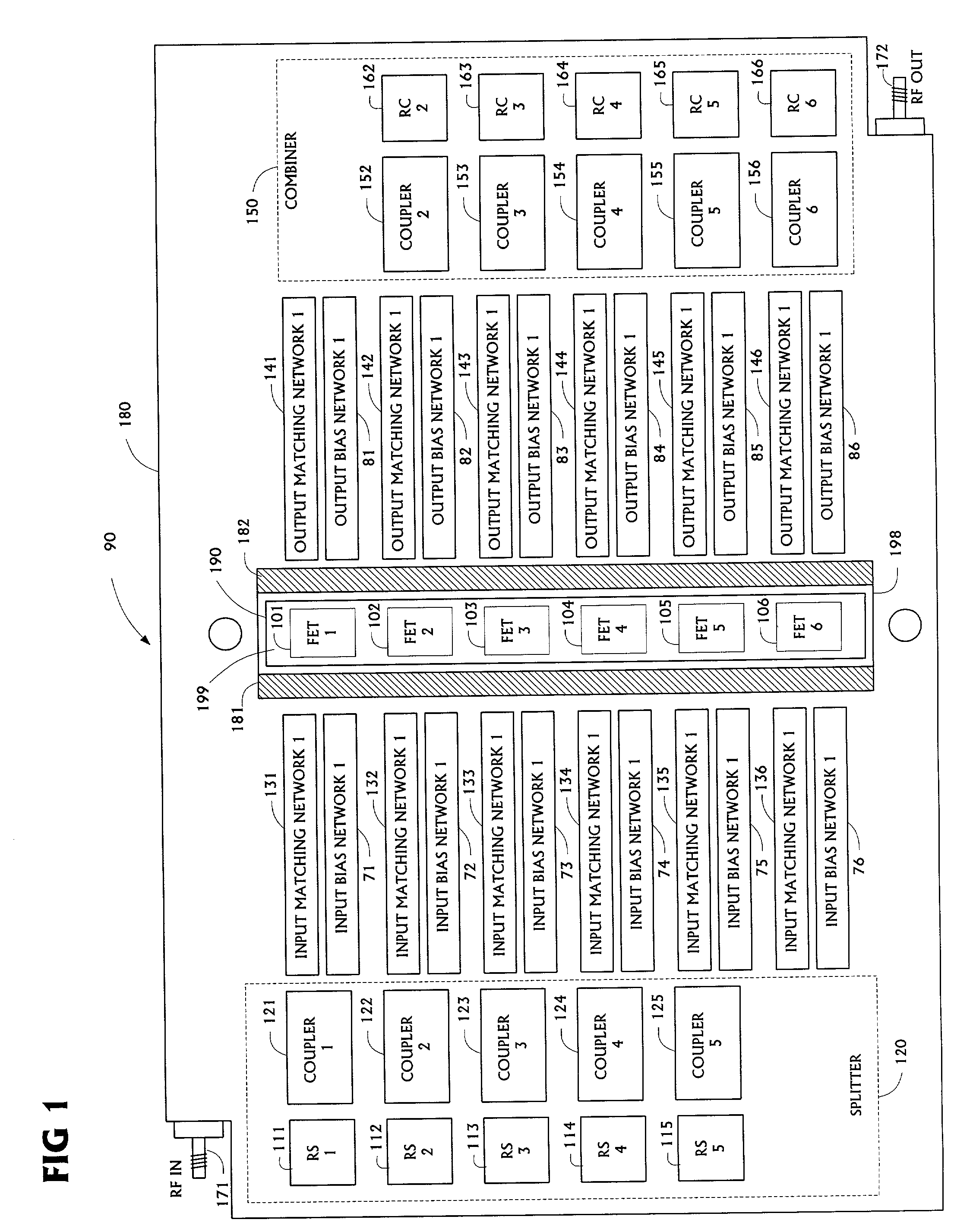
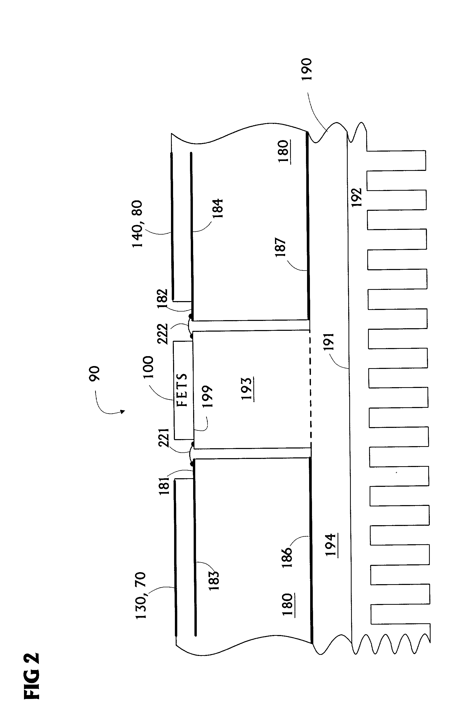
[0018] FIG. 1 illustrates a combined functional / physical layout of a high frequency, high power ("broadband") broadband amplifier 90 constructed in accordance with one aspect of the invention. The amplifier 90 generally includes a printed circuit board (PCB) 180 and a power transistor pedestal 190. The PCB 180 has as RF power input 171 for receiving a RF input signal, and a RF power output 172 for outputting an amplified RF output signal. The pedestal 190 has a surface 199 with a plurality of power transistor circuits ("power transistors") 101-106 attached thereto. The power transistors 101-106 each amplify a phase component signal of the RF input signal to thereby boost the power level from the RF power input 171 to the RF power output 172.

[0019] The pedestal 190 provides support for the circuit components of the respective power transistors 101-106; provides a high electrical conductivity for carrying common currents; and provides high thermal conductivity for cooling. One preferr...


PUM


Abstract

A broadband RF signal amplifier includes a plurality of transistors attached to a surface of a pedestal, each transistor having an input and an output. An RF input path electrically connected to the transistor inputs includes a passive splitter implemented in a multi-layer printed circuit board and configured to split a RF input signal into a plurality of component input signals. A plurality of corresponding input matching networks including one-quarter wavelength transmission lines implemented in the printed circuit board couple respective component input signals to the transistor inputs at an input impedance, the input matching networks further comprising respective input matching capacitors attached to the pedestal. An RF output path electrically connected to the transistor outputs includes a passive combiner implemented in the printed circuit board and configured to combine component output signals received at the transistor outputs into a RF output signal. A plurality of corresponding output matching networks including one-quarter wavelength transmission lines implemented in the printed circuit board couple the respective component output signals at the transistor outputs to an output impedance.

Description

[0001] The present invention pertains generally to the field of radio frequency (RF) power transistor devices and, more specifically, to high frequency, high power signal amplifiers used in wireless communication applications.[0002] The use of RF power transistor devices as signal amplifiers in wireless communication applications is well known. With the recent growth in the demand for wireless services, such as personal communication services, the operating frequency for wireless networks has increased dramatically and is now well into the gigahertz. For example, RF power transistors are commonly used in amplification stages for radio base station amplifiers in wireless communication networks. Such power transistors are also widely used in other RF-related applications, such as cellular telephones, paging systems, navigation systems, television, avionics, and military applications.[0003] Production of RF power transistors on a large-volume basis is traditionally problematic, because...

Claims


Application Information

Patent Timeline
IPC IPC(8): H01L23/48H01L23/66H03F3/60
CPCH01L23/48H01L23/66H01L2924/1306H01L2924/01072H01L2924/01068H01L24/49H01L2223/6644H01L2223/665H01L2224/32188H01L2224/48091H01L2224/49175H01L2924/01013H01L2924/01029H01L2924/01082H01L2924/19041H01L2924/19042H01L2924/19043H01L2924/30105H01L2924/30107H01L2924/3011H01L2924/3025H03F3/604H01L24/48H01L2924/01033H01L2924/00014H01L2924/00H01L2924/30111H01L2224/45099
Inventor MOLLER, THOMAS W.LEIGHTON, LARRYPERUGUPALLI, PRASANTH
Owner INFINEON TECH AG
Why Eureka
Try Eureka