Silicon wafer and epitaxial silicon wafer

a technology of epitaxial silicon and silicon wafer, which is applied in the field of epitaxial silicon wafer and silicon wafer, can solve the problems of increasing leakage current, deterioration of electric characteristics, and increasing quality standards of silicon wafers on which devices are formed

Inactive Publication Date: 2003-06-05
SUMITOMO MITSUBISHI SILICON CORP
View PDF7 Cites 42 Cited by
  • Summary
  • Abstract
  • Description
  • Claims
  • Application Information

AI Technical Summary

Problems solved by technology

In recent years, the tendency toward higher degree of integration of silicon semiconductor integrated circuit devices has been rapidly increasing and, accordingly, silicon wafers on which devices are formed have been subjected to increasingly severe quality standards.
Therefore, in manufacturing highly integrated devices, it is necessary to employ the so-called gettering technology which comprises trapping metal impurities at a site (in a sink) remote from the device active region, since the occurrence of crystal defects or metal impurities other than a dopant in the device active region where devices are to be formed leads to deterioration in electric characteristics, for example an increase in leakage current.
It is generally well known that, in p-type silicon wafers doped with boron (B) or the like, crystal defects including oxygen precipitates due to supersaturated interstitial oxygen, dislocations, and stacking faults, are ind

Method used


Image

  • Silicon wafer and epitaxial silicon wafer
  • Silicon wafer and epitaxial silicon wafer

Examples


example 1

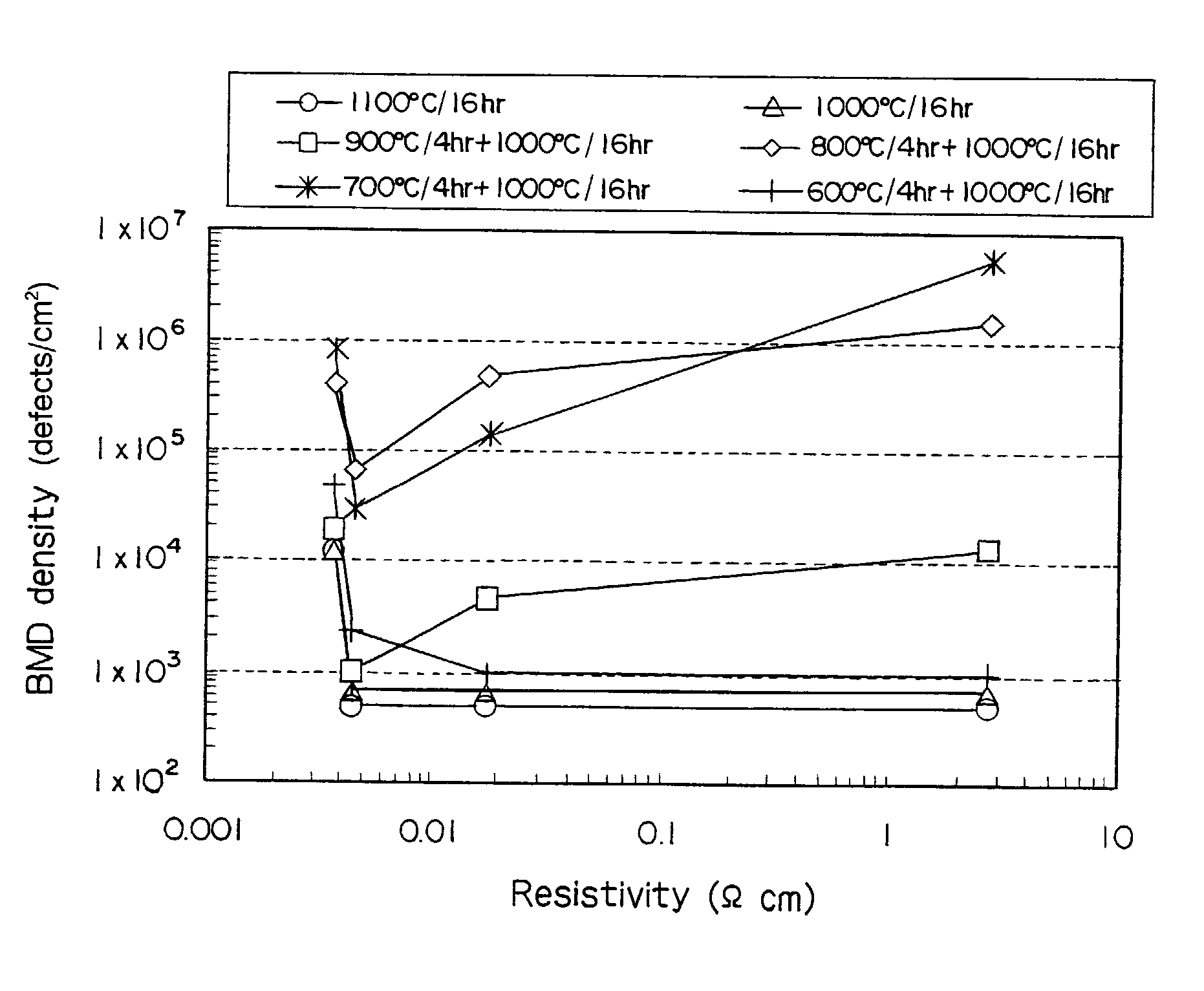
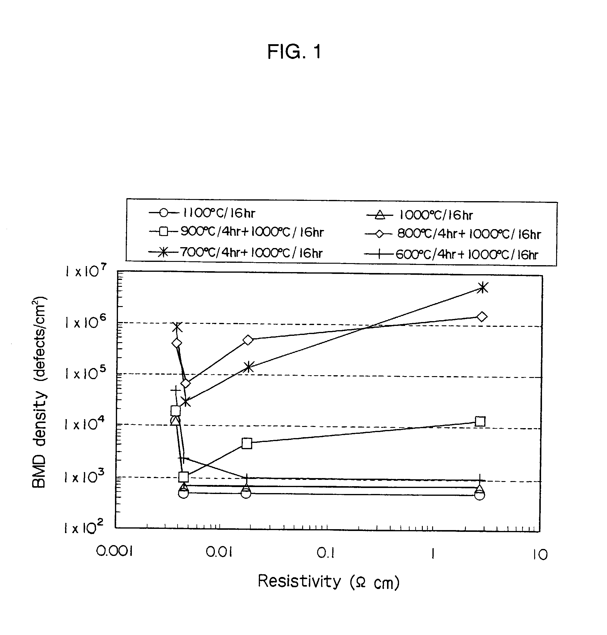
[0045] For examining the efficacy of nitrogen addition in arsenic-doped n-type silicon wafers, silicon wafers were prepared while varying the arsenic addition level and nitrogen concentration and, after evaluation heat treatment, each wafer was measured for wafer inside BMD density.

[0046] Specifically, silicon single crystals having an initial oxygen concentration of 11.5 to 18.5.times.10.sup.17 atoms / cm.sup.3 (ASTM F 121-79), a crystal orientation of (100) and a diameter of 150 mm were grown by the Czochralksi method from silicon melts while the arsenic addition level was varied to give a resistivity within the range of 0.018 .OMEGA.cm to 0.003 .OMEGA.cm and, simultaneously, the nitrogen concentration was varied.

[0047] Wafers were sliced from each silicon single crystal, and mirror polished sample wafers were prepared therefrom. Each sample wafer was subjected to evaluation heat treatment, namely isothermal heat treatment under conditions of 1,100.degree. C. (heating) / 16 hours (mai...

example 2

[0049] For examining the efficacy of nitrogen addition in epitaxial silicon wafers derived from arsenic-doped n-type silicon wafers by forming epitaxial layer, silicon wafers were prepared while varying the arsenic addition level and nitrogen concentration, and the silicon wafers were subjected to epitaxial growing treatment. The thus-produced epitaxial silicon wafers were subjected to evaluation heat treatment and then measured for the density of BMDs formed in the wafer inside. Epitaxial silicon wafers derived from the silicon wafers subjected to heat treatment for forming oxygen precipitates prior to epitaxial growing treatment were also measured for BMD density.

[0050] Specifically, silicon single crystals having an initial oxygen concentration of 8 to 18.5.times.10.sup.17 atoms / cm.sup.3 (ASTM F 121-79), a crystal orientation of (100) and a diameter of 150 mm were grown by the Czochralksi method from silicon melts while the arsenic addition level was varied to give a resistivity ...


PUM


Abstract

The invention relates to a silicon wafer and an epitaxial silicon wafer, which are doped with arsenic (As) as an n-type dopant and are excellent in gettering characteristics. A first silicon wafer has a resistivity of 10 OMEGAcm to 0.001 OMEGAcm as a result of addition of arsenic and has a nitrogen concentration of 1x10¹³ to 1x10¹⁵ atoms/cm3. A second silicon wafer has a resistivity of 0.1 OMEGAcm to 0.005 OMEGAcm and a nitrogen concentration of 1x10¹⁴ to 1x10¹⁵ atoms/cm3. A third silicon wafer has a resistivity of 0.005 OMEGAcm to 0.001 OMEGAcm and a nitrogen concentration of 1x10¹³ to 3x10¹⁴ atoms/cm3. An epitaxial silicon wafer derived from any of the first to third silicon wafers by forming an epitaxial layer in the surface layer portion is provided. In producing this epitaxial silicon wafer, epitaxial layer formation is desirably carried out after subjecting the silicon wafer to heat treatment for forming oxygen precipitates under conditions of a temperature not lower than 700° C. but lower than 900° C. and a period of 30 minutes to 4 hours. By these, an oxygen precipitate density can be secured and a sufficient gettering effect can be produced in the device producing process in spite of their being n-type silicon wafers doped with a high concentration of arsenic.

Description

[0001] The present invention relates to a silicon wafer and an epitaxial silicon wafer, which are to be used for the manufacture of semiconductor integrated circuit devices and, more particularly, to a silicon wafer and an epitaxial silicon wafer, which contain arsenic (As) added as an n-type dopant and are excellent in gettering characteristics.DESCRIPTION OF THE PRIOR ART[0002] In recent years, the tendency toward higher degree of integration of silicon semiconductor integrated circuit devices has been rapidly increasing and, accordingly, silicon wafers on which devices are formed have been subjected to increasingly severe quality standards. Therefore, in manufacturing highly integrated devices, it is necessary to employ the so-called gettering technology which comprises trapping metal impurities at a site (in a sink) remote from the device active region, since the occurrence of crystal defects or metal impurities other than a dopant in the device active region where devices are t...

Claims


Application Information

Patent Timeline
IPC IPC(8): C30B29/06C30B15/00H01L21/205H01L21/322
CPCC30B15/00Y10T428/26H01L21/3225C30B29/06
Inventor ONO, TOSHIAKIHORAI, MASATAKA
Owner SUMITOMO MITSUBISHI SILICON CORP
Why Eureka
Try Eureka