Semiconductor laser module and Raman amplifier

a laser module and amplifier technology, applied in semiconductor lasers, electromagnetic repeaters, instruments, etc., can solve problems such as noise accumulation, signal distortion and noise generation, and increase in data traffic as a problem

Inactive Publication Date: 2003-07-10
FURUKAWA ELECTRIC CO LTD
View PDF6 Cites 18 Cited by
  • Summary
  • Abstract
  • Description
  • Claims
  • Application Information

AI Technical Summary

Problems solved by technology

Following the recent rapid spread of the Internet and the rapid increase of in-company LAN connection, an increase in data traffic appears as a problem.
The EDFA has, therefore, restrictions which include noise accumulation due to the loss of a transmission optical fiber, and signal distortion and noise generation due to the non-linearity of a transmission optical fiber.
In addition, since the EDFA enables amplifying light in a wavelength band only set by the Er band gap energy, it is difficult to widen band to realize further multiplexing.
This Raman gain fluctuation results in fluctuation in the intensity of an amplified signal, which disadvantageously hampers Raman amplification.
This Raman gain fluctuation results in the fluctuation of the amplified signal intensity, which disadvantageously hampers stable Raman amplification.
To do so, it takes time and labor for optical axis alignment during assembly.
In addition, since this optical coupling is mechanical optical couplin

Method used


Image

  • Semiconductor laser module and Raman amplifier
  • Semiconductor laser module and Raman amplifier
  • Semiconductor laser module and Raman amplifier

Examples


first embodiment

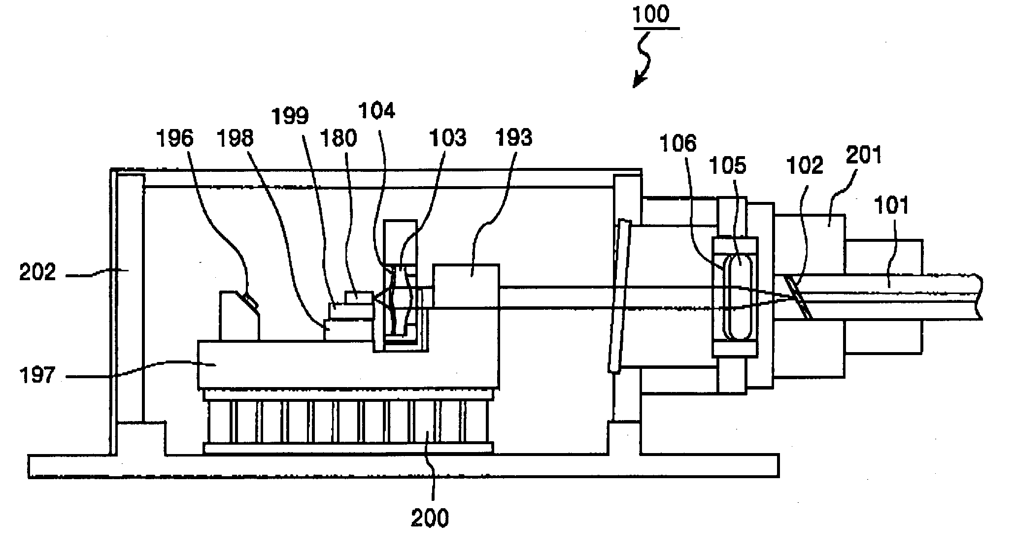
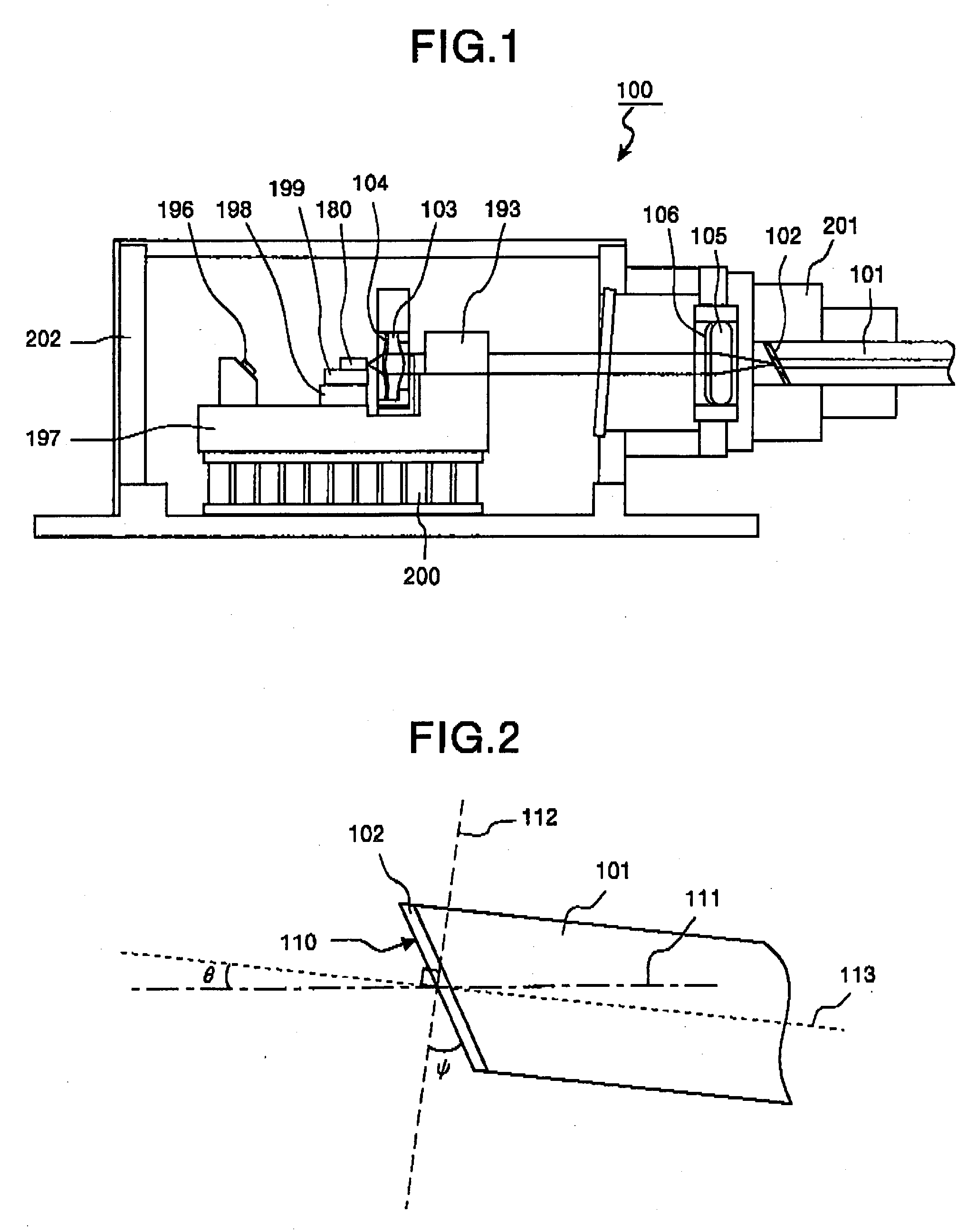
[0056] FIG. 1 is a longitudinal sectional view which shows the configuration of the semiconductor laser module according to the In FIG. 1, components as same or similar structures or functions as those shown in FIG. 19 are denoted by the same reference numerals, and in order to avoid redundancy, are not be explained. A semiconductor laser module 100 shown in FIG. 1 differs from the semiconductor laser module 103 shown in FIG. 9 in that a first lens 103 which has a non-reflection coating 104 formed on a laser beam incident surface is provided in place of the first lens 192, a second lens 105 which has a non-reflection coating 106 formed on a laser beam incident surface is provided in place of the second lens 194 and an optical fiber 101 having a laser beam incident surface, which is askew to an optical axis and which has a non-reflection coating 102 formed thereon, is provided in place of the optical fiber 203 which has the laser beam incident end surface perpendicular to the optica...

second embodiment

[0070] FIG. 6 is a longitudinal sectional view which shows the configuration of the semiconductor laser module according to the In FIG. 6, components having same or similar structure or function as those shown in FIG. 1 have been denoted by the same reference numerals, and to avoid repetition of explanation, their explanation will be omitted. The semiconductor laser module 300 shown in FIG. 6 differs from the semiconductor laser module 100 shown in FIG. 1 in that a semiconductor laser device 20 to be explained later is provided in place of the Fabry-Perot type semiconductor laser device 180.

[0071] The structure and feature of the semiconductor laser device 20 will be explained. FIG. 7 is a perspective broken-out view which shows the schematic configuration of a semiconductor laser device in the semiconductor laser module according to the second embodiment. FIG. 8 is a longitudinal sectional view of the semiconductor laser device shown in FIG. 7. FIG. 9 is a cross-sectional view tak...


PUM


Abstract

A semiconductor laser module has a Fabry-Perot type semiconductor laser device, an optical fiber, and first and second lenses. The tip of the optical fiber, on which the laser beam falls, is askew polished. The optical fiber is fixed in such a manner that the axis of the optical fiber makes an angle with respect to an optical axis of the laser beam. Coatings that avoid reflection are formed on the tip of the optical fiber, and on the first and second lenses.

Description

[0001] 1) Field of the Invention[0002] The present invention relates to a semiconductor laser module and a Raman amplifier that has reduced relative intensity noise (RIN).[0003] 2) Description of the Related Art[0004] Following the recent rapid spread of the Internet and the rapid increase of in-company LAN connection, an increase in data traffic appears as a problem. A dense-wavelength division multiplexing (DWDM) transmission system which has been developed to prevent a decrease in communication performance due to increased data traffic is spreading fast.[0005] The DWDM transmission system realizes a large capacity transmission that transfers 100 times larger signal than the conventional system by carrying multiple optical signals on different wavelengths on a single fiber. The existing DWDM transmission system particularly enables wideband, long-distance transmission using an erbium-doped fiber amplifier (EDFA). The EDFA, Er-doped optical fiber, amplifies signals with the wavelen...

Claims


Application Information

Patent Timeline
IPC IPC(8): G02B6/42G02F1/35H01S3/094H01S3/10H01S3/30H01S5/024H01S5/12H01S5/34H04B10/2507H04B10/29H04B10/294
CPCB82Y20/00H01S2301/02H01S3/094011H01S3/302H01S5/02248H01S5/02284H01S5/02296H01S5/02415H01S5/0683H01S5/1092H01S5/12H01S5/146H01S5/227H01S5/3408G02B6/4206H01S5/02257H01S5/02325H01S5/02251
Inventor SHIMIZU, HIROSHITSUKIJI, NAOKIYOSHIDA, JUNJIKIMURA, TOSHIOOHKI, YUTAKATERADA, KOUHEITANIGUCHI, HIDEHIRO
Owner FURUKAWA ELECTRIC CO LTD
Why Eureka
Try Eureka