Low resistance conductor, processes of production thereof, and electrical members using same
a low-resistance conductor and process technology, applied in the direction of conductors, superconducting magnets/coils, magnetic bodies, etc., can solve the problems of insufficient critical current density, inability to obtain larger materials than this, and limited material production limits, etc., to achieve low specific resistance, low cost, and easy handling
- Summary
- Abstract
- Description
- Claims
- Application Information
AI Technical Summary
Benefits of technology
Problems solved by technology
Method used
Image
Examples
example 2
[0175] Changing only the Y.sub.2O.sub.3 in the source powder to Dy.sub.2O.sub.3, the same method as in Example 1 was used to prepare a Dy-based bulk material. This was sliced to a thickness of 0.6 mm, then processed to bar-shaped materials such as shown in FIG. 14 and bar-shaped materials having curved and bent shapes such as shown in FIG. 16(a) and FIG. 16(b).
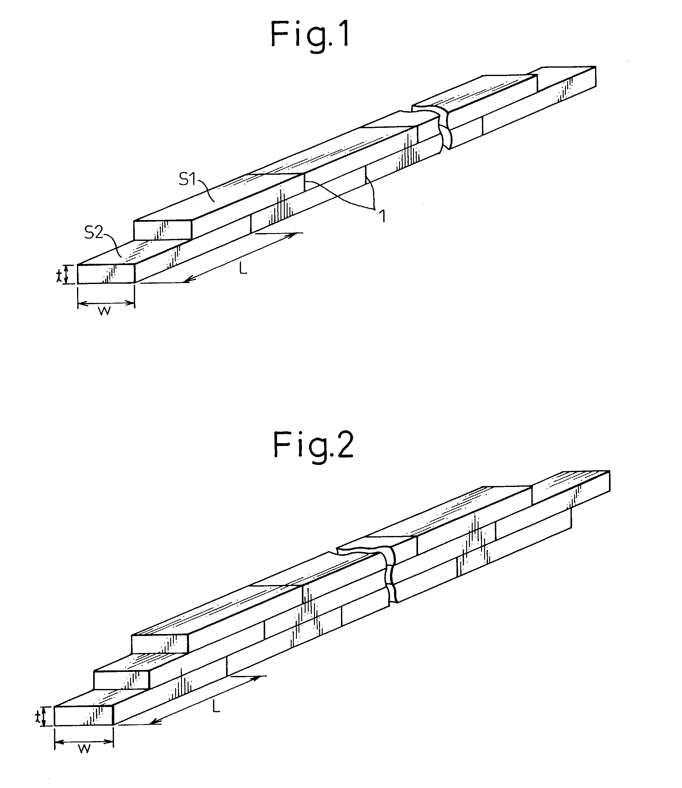
[0176] These were coated with silver on their surfaces in the same way as with Example 1, then assembled to prepare L-shaped low resistance conductors of total lengths of about 1 m. At this time, the superconductors were connected with each other in the arrangement shown in FIG. 1 in the same way as in Example 1 using solder. At the connections at this time, the coating layers of silver were 5 .mu.m thick and the solder layers were about 50 .mu.m thick.
[0177] 500A of current was passed through the above two types of low resistance conductors to measure the resistances, whereupon they were found to be both approximately 1.3.tim...
example 3
[0179] The ends of a low resistance conductor 8 prepared in Example 1 were connected with copper electrodes, then the conductor was given an insulation coating 5, then inserted into a triple pipe as shown in FIG. 17(a). The end where the triple pipe is connected in series (comprised of the flange 9 and O-ring 10) had the structure shown in FIG. 17(b). This had the copper electrode 11 insulated from the surroundings and the liquid nitrogen channels 6 and 12 covered by a vacuum heat insulating layer 7.
[0180] Five of these cables 13 were connected in series and a load 15 and DC power source 14 connected so as to prepare the power feed experimental circuit shown in FIG. 18. 500A was passed through the load 15, whereupon the power transmission loss occurring in one cable was about 3.2W. Compared with the loss at room temperature of a copper wire having a thickness of the cable (outside diameter of triple pipe) (about 120W), it was possible to reduce the loss to about {fraction (1 / 40)}th ...
example 4
[0181] The methods described in Example 1 and Example 2 were used to prepare Y-based and Dy-based approximately 46 mm diameter columnar bulk materials. These were sliced to 1.0 mm thicknesses, then straight bar-shaped materials and 45 degree angle bent bar-shaped materials of widths of 1.9 mm were prepared from the Y-based material and of 2.2 mm were prepared from the Dy-based material. These were coated with silver, then infused with oxygen by the annealing method described in Example 1.
[0182] These were electrically connected by solder. At this time, the thicknesses of the solder layers were about 60 .mu.m. Further, the thicknesses of the silver coatings were 5 .mu.m.
[0183] Pancake coils (innermost diameter of 62 mm and outermost diameter of 138 mm) comprised of five turns of the 2.2 mm width conductor at the inside and 8 turns of the 1.9 mm width conductor at the outside were prepared by connecting bent members 16 and bar-shaped members 17 in the arrangements shown in FIG. 19(a) ...
PUM
| Property | Measurement | Unit |
|---|---|---|
| thickness | aaaaa | aaaaa |
| thickness | aaaaa | aaaaa |
| thickness | aaaaa | aaaaa |
Abstract
Description
Claims
Application Information


