As integrated circuits ("ICs") have become progressively more microminiaturized to provide higher computing speeds, current dielectric materials used in the manufacturing of the ICs have proven to be inadequate in several ways.
These materials, for instance, have high dielectric constants, difficulty to use in the manufacturing process, have inadequate
thermal instability and generate toxic by-products.
Corrosive organic elements used for IC
processing can cause interfacial
corrosion of the barrier material, and it is essential that the dielectric material does not allow the organic elements to diffuse into the barrier material layer.
Current
solid materials are unable to achieve stability, integrity and strength with a dielectric constant below 2.7.
However, the average void sizes in a cross-section of a well prepared "pin-hole free" or "
solid" films are only few Angstroms.
However, when the sacrificing materials have different compatibilities with the
polymer matrix, the result can lead to
polymer aggregation and pore sizes larger than 100 Angstroms.
The resulting thin film dielectric has poor mechanical properties due to localized degradation caused by large pores or their aggregates.
The presence of pores in these dielectric materials normally results in holes on newly formed surfaces, thus making subsequent depositions of a continuous, thin (<50-100 .ANG.) barrier
layers and
copper seed
layers very difficult if not impossible.
Additional problems with traditional
porous thin films are they often exhibit reliability problems due to the inclusion of barrier
metal inside the
dielectric layer, as occurs after PVD of Ta.
Porous dielectric materials are also difficult to integrate into IC fabrications that involve a CMP process.
To further complicate the process, large surface areas in porous films lead to high water adsorption that can limit the electrical reliability of the IC.
Unfortunately, the porous BCB and other dielectric materials that can achieve a .epsilon..ltoreq.2.4 are too soft for CMP and not suitable for fabrication of current and future ICs.
However, despite its
low leakage current due to presence of sp.sup.3C--F bonds, a low
thermal stability occurred due to presence of sp.sup.3 C--F and sp.sup.3C-sp.sup.3-C bonds in the films.
Thus, these
fluorinated polymers are unable to withstand the prolonged high temperatures necessary for IC manufacture.
However, in
spite of the low dielectric constant, these
polymer films also had a low
thermal stability due to presence of sp.sup.3C-sp.sup.3C and sp.sup.3C--F bonds in these films.
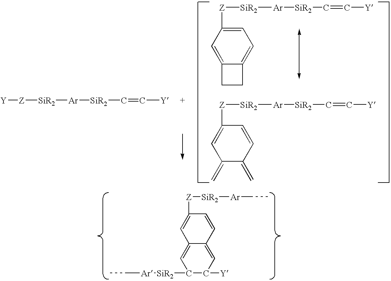
However, there are disadvantages to the known methods the manufacture of the fluorinated poly (Para-Xylylenes), or
Parylene AF.sub.4.TM.. First, the manufacture of their precursors is inefficient because the chemical reactions have low yields, and the process is expensive and produces toxic byproducts.
Further, it is difficult to eliminate redimerization of the reactive intermediates.

