

Production method of laminate ceramic electronic component
a technology of electronic components and laminate ceramics, which is applied in the direction of fixed capacitors, emergency protective circuit arrangements, emergency protection arrangements for limiting excess voltage/current, etc., can solve the problems of high cost of produced capacitors, prone to cracks (particularly, inner cracks) in obtained capacitors, and oxidized base metal reduction, improvement effect, and increase dielectric constant
- Summary
- Abstract
- Description
- Claims
- Application Information
AI Technical Summary
Benefits of technology
Problems solved by technology
Method used
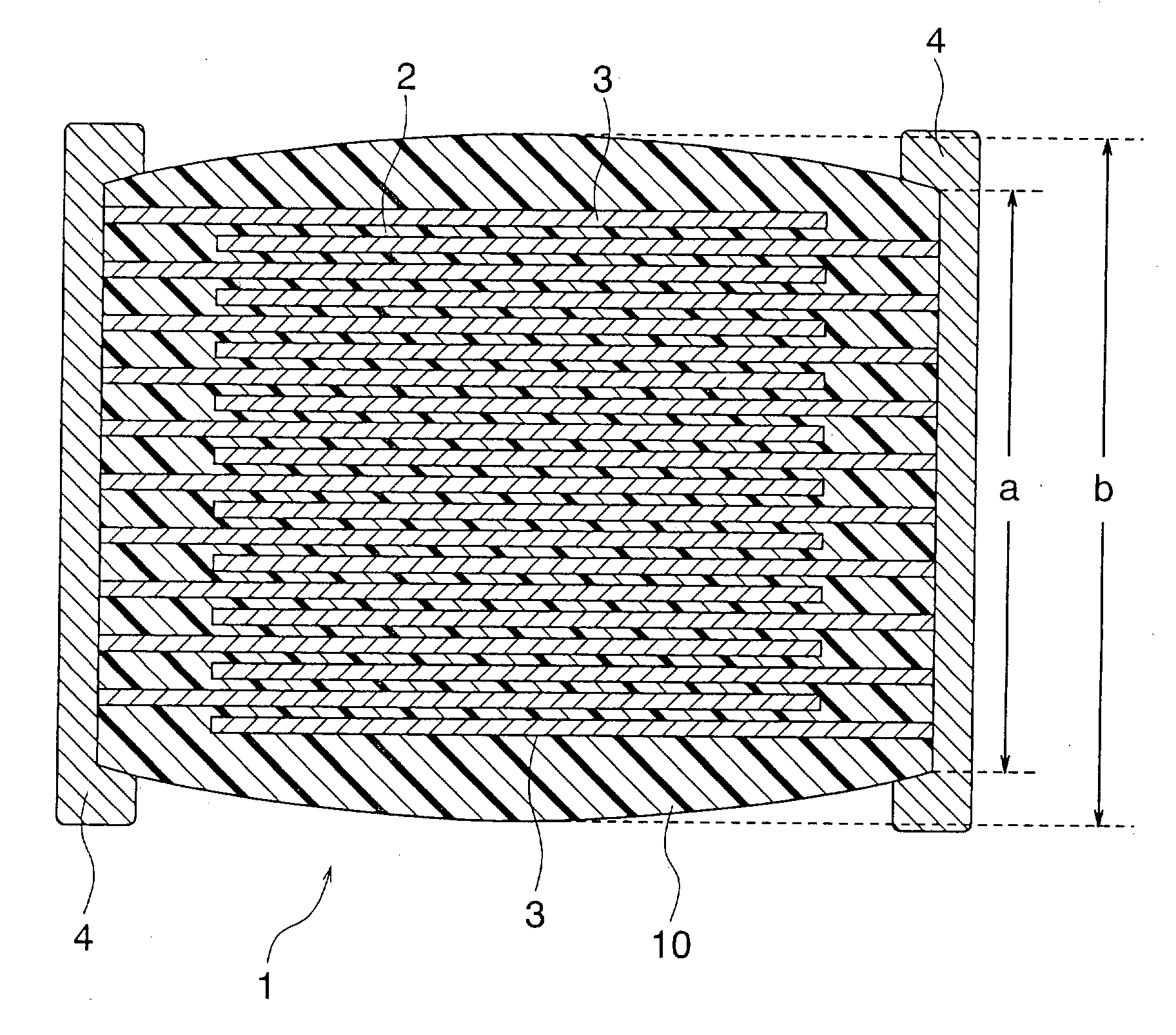
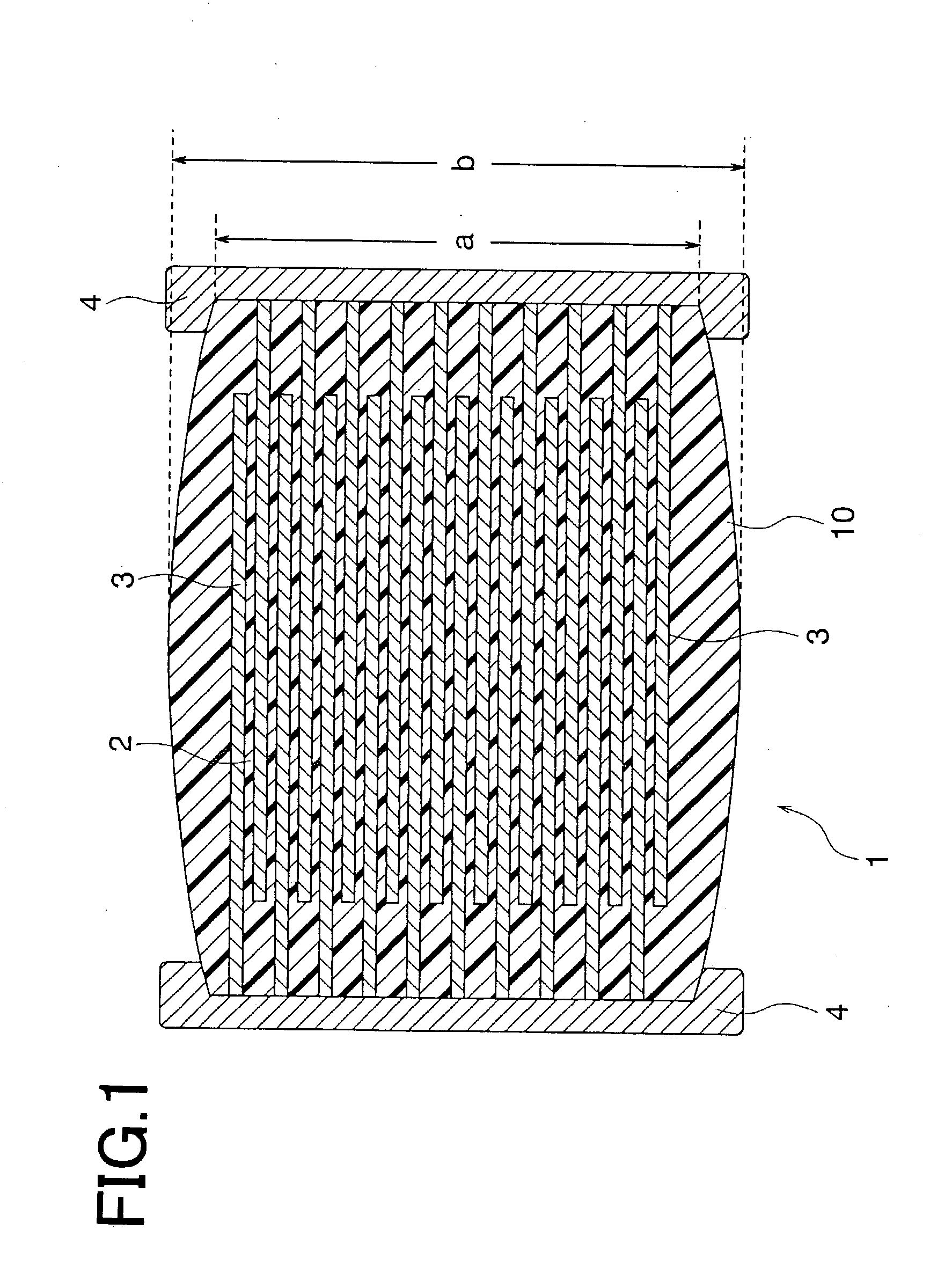
Image

Examples
example 2
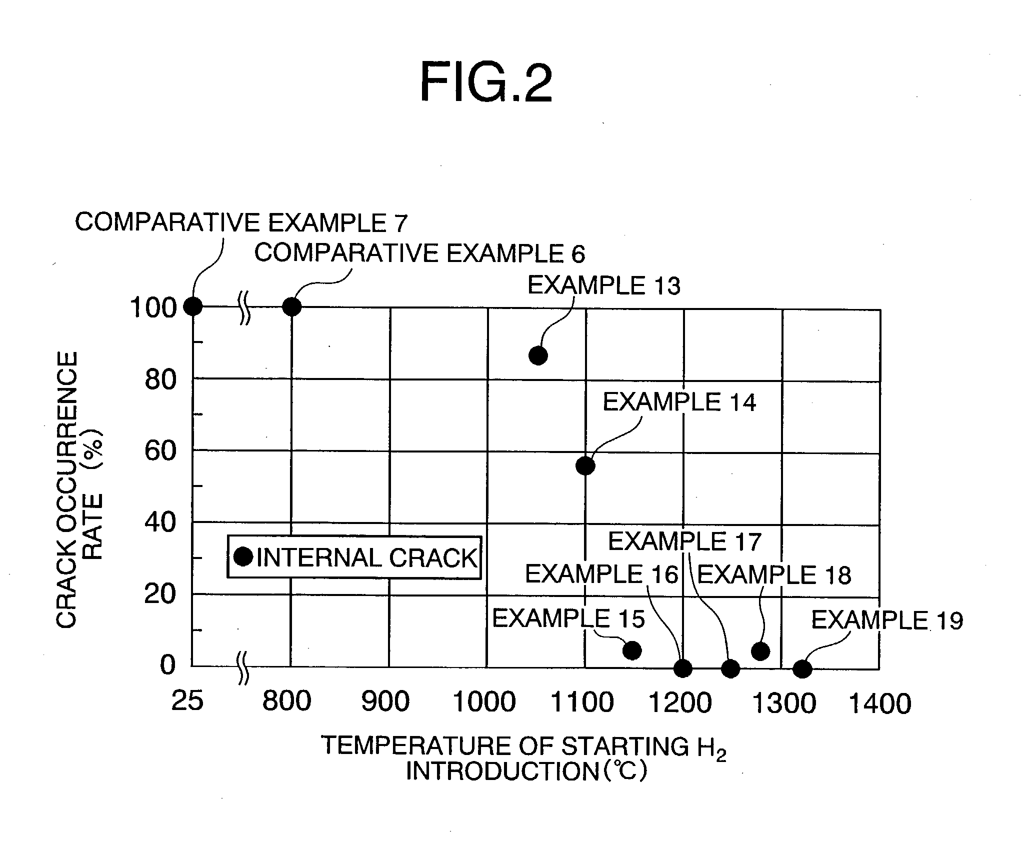
[0150] Capacitor samples were obtained in the same way as in the Example 1 except that hydrogen introduction was started at the time the temperature was raised to 1150.degree. C. in the firing step. Evaluation was made in the same way as in the Example 1.
[0151] As a result, the static capacitance of the obtained capacitor samples was 15 .mu.F and the capacity was confirmed to be increased comparing with the Example 1. The defective fraction of insulation resistance (IR) of the capacitor samples was 0% and the IR defective fraction was confirmed to be drastically improved comparing with the Example 1. The shape anisotropy of the capacitor samples was ".largecircle." and no shape anisotropy was observed.
example 3
[0152] Capacitor samples were obtained in the same way as in the Example 1 except that hydrogen introduction was started at the time the temperature was raised to 1220.degree. C. in the firing step. Evaluation was made in the same way as in the Example 1.
[0153] As a result, the static capacitance of the obtained capacitor samples was 14 .mu.F and the capacity was increased comparing with the Example 1. While, when comparing with the Example 2, a little decrease in the capacity was confirmed. The reason is not exactly clear, but it is deemed that it is because when hydrogen introduction starts at the time of reaching the firing temperature, sintering of the dielectrics tends to be insufficient, and thereby, the capacity decreases. The defective fraction of insulation resistance (IR) of the capacitor samples was 0% and the IR defective fraction was confirmed to be drastically improved comparing with the Example 1. The shape anisotropy of the capacitor samples was ".largecircle." and n...
example 4
[0158] Capacitor samples were obtained in the same way as in the Example 1 except that the number of dielectric layers sandwiched between two internal electrode layers was 500. Evaluation was made in the same way as in the Example 1.
[0159] As a result, the static capacitance of the obtained capacitor samples was 74 .mu.F. The defective fraction of insulation resistance (IR) of the capacitor samples was 50%. The shape anisotropy of the capacitor samples was ".largecircle." and no shape anisotropy was observed.
PUM
| Property | Measurement | Unit |
|---|---|---|
| temperature | aaaaa | aaaaa |
| temperature | aaaaa | aaaaa |
| temperature | aaaaa | aaaaa |
Abstract
Description
Claims
Application Information