Functional optical module
a technology of optical modules and optical modules, applied in the field of functional optical modules, can solve the problems of large capacity of the entire device, the length of the device is a few cm, and the capacity of the problem
Inactive Publication Date: 2003-08-14
FURUKAWA ELECTRIC CO LTD
View PDF12 Cites 32 Cited by
- Summary
- Abstract
- Description
- Claims
- Application Information
AI Technical Summary
Benefits of technology
[0021] Further, in the case of an optical connector such that fiber guides are provided in parallel on a chip produced using a semiconductor production technique, it is difficult to attach an optical fiber to a fiber guide. Moreover, it is required to carefully handle an optical fiber removed from a chip to prevent occurrences of breakage and insertion loss of optical fiber in assembly.
[0049] In view of the foregoing, it is an object of the third invention to provide an optical switch compact in size and greatly easy in handling and assembly
Problems solved by technology
However, following problems exist in using the above-mentioned conventional collimator, optical functional component, and functional optical module provided with the collimator and component in a DWDM (Dense Wavelength Division Multiplexing) communication scheme.
In this case, since a single optical functional component has a size to some extent, the entire device occupies an enormously large capacity.
With respect to an AWG (Array Wave Guide Grating) wavelength division multiplexing device, although various components are integrated on a single chip, the device is a few cm in length currently, and has problems with its capacity.
Further, in the case of an optical connector such that fiber guides are provided in parallel on a chip produced using a semiconductor production technique, it is difficult to attach an optical fiber to a fiber guide.
In order to permanently prevent such occurrences of breakage and addition loss of optical fiber, it is required to provide a protecting member such as a housing to protect components from dusts in the air, resulting in problems that production processes become more complicated and production facilities are upsized.
The AWG wavelength division multiplexing device has also has such problems; it is difficult to connect each waveguide and an optical fiber and handle the optical fiber.
Furthermore, low dimensional accuracy of a lens causes deviations in position and direction of an optical axis of a light beam, thus disabling predetermined functions.
The above problems do not arise in using the above-mentioned optical fiber collimator composed of an SM fiber with a GI fiber fusion-spliced in its front end, but such an optical fiber collimator has following problems.
For example, in the case of a laser light emitting device, when optical properties of a laser light emitting device are not coincident with optical properties of a lens, the optical function is not exhibited properly, nor predetermined effects are not obtained.
This process includes complicated operations such as removing a protecting member and aligning an optical axis of optical fiber, puts an enormous load on its supplier in cost, facilities and operation efficiency, and is virtually impossible to execute.
However, there have been following problems with the above-mentioned conventional technique.
First, since the reception electrode of the optical functional component and the power supply electrode of the housing are connected by boding, when the need arises of exchanging the optical functional component with another optical functional component with a different function, it is necessary to open the housing, remove the bonded wires, dispose a new optical functional component, and perform bonding again, and thus an enormous load is put on its supplier.
Furthermore, a general capillary for bonding is configured to operate upwardly and downwardly, which results in that the reception electrode is provided upwardly, and it is difficult to produce a sideward optical functional component.
However, electrode formation in the semiconductor production process is generally performed by deposition or sputtering, and in order to form a reception electrode on a side face of each component by the deposition or sputtering, a step of rearranging a number of components is necessary so that a side face of each of the components becomes a target for the deposition or sputtering, which puts an enormous load on the supplier in cost, apparatus and process, and is virtually impossible to implement.
However, the component sensitive to heat and / or vibration restricts heating condition and / or ultrasonic condition, and there arises a case that the electrode cannot be fixed with reliability.
Further, since the wiring for use in boding is generally composed of a fine metal line with approximately few .mu.m, a break may occur in the wiring due to fine dusts, dirt and / or wind.
First, it is very difficult to connect an optical fiber and the switch. For example, in the method of moving a mirror on a substrate, since a light beam is reflected by the mirror, it is required to enhance accuracy in arrangement of the optical fiber and mirror. Therefore, the switch is often provided with a V-shaped groove on which an optical fiber is placed.
However, there is a risk that the optical fiber escapes from the V-shaped groove when the V-shaped groove is covered, and highly precise assembly is required.
However, when a fiber collimator is used, the fusion may cause fluctuations in refractive index distribution of a GI fiber, and it is not possible to obtain a desired form for characteristics of collimator, thus resulting in increased insertion loss.
To implement such a distance between the end faces, it is necessary to provide the fiber with a specialized process to taper a front end of the fiber, and thus the extremely complicated process is required.
Further, in the optical switch disclosed in JP 2000-98270, its configuration makes it difficult to align the fiber collimator and reflector, and there arises a risk of introducing an optical loss.
Furthermore, as described above, since there are a large number of parts composing the optical switch which are provided independently of each other, complicated assembly and alignment adjustments for the parts are needed.
Then, in the conventional optical switch with a configuration in which a waveguide type refractive index matching member is inserted and removed at an intersection portion of waveguides, there are problems that the operation speed is low and thus the practicality is low, and that a coupling loss of optical fibers of a rectangle waveguide and of a circular waveguide is increased as compared to a coupling loss of circular waveguides (optical fibers) and thus the practicality deteriorates.
Method used
View moreImage
Smart ImageViewing Examples
Examples
sixth embodiment
[0062] the first invention is a functional optical module in which the collimator lens has anti-reflection coating on an end face portion at its one side or both sides.
seventh embodiment
[0063] the first invention is a functional optical module in which the collimator lens is made of a graded index fiber.
eighth embodiment
[0064] the first invention is a functional optical module in which the optical functional component is an optical attenuator.
Login to View More PUM
 Abstract
The invention comprises three parts: The first parts provides a miniaturized functional optical module, which is provided with a lens-exchange type collimator enabling rapid and easy exchange of an optical functional component and / or lenses and being compact in size and excellent in durability. The second part provides a power supply device for an optical functional component that supplies power to the optical functional component with reliability for a long term and enables easy exchange of the optical functional component, and an optical functional module having such a power supply device. The third part provides an optical switch compact in size and greatly easy in handling, which is provided with a connector module having a plurality of optical fibers for light-beam input, a plurality of optical fibers for light-beam output corresponding to the plurality of optical fibers and a light-beam reflecting member.
Description
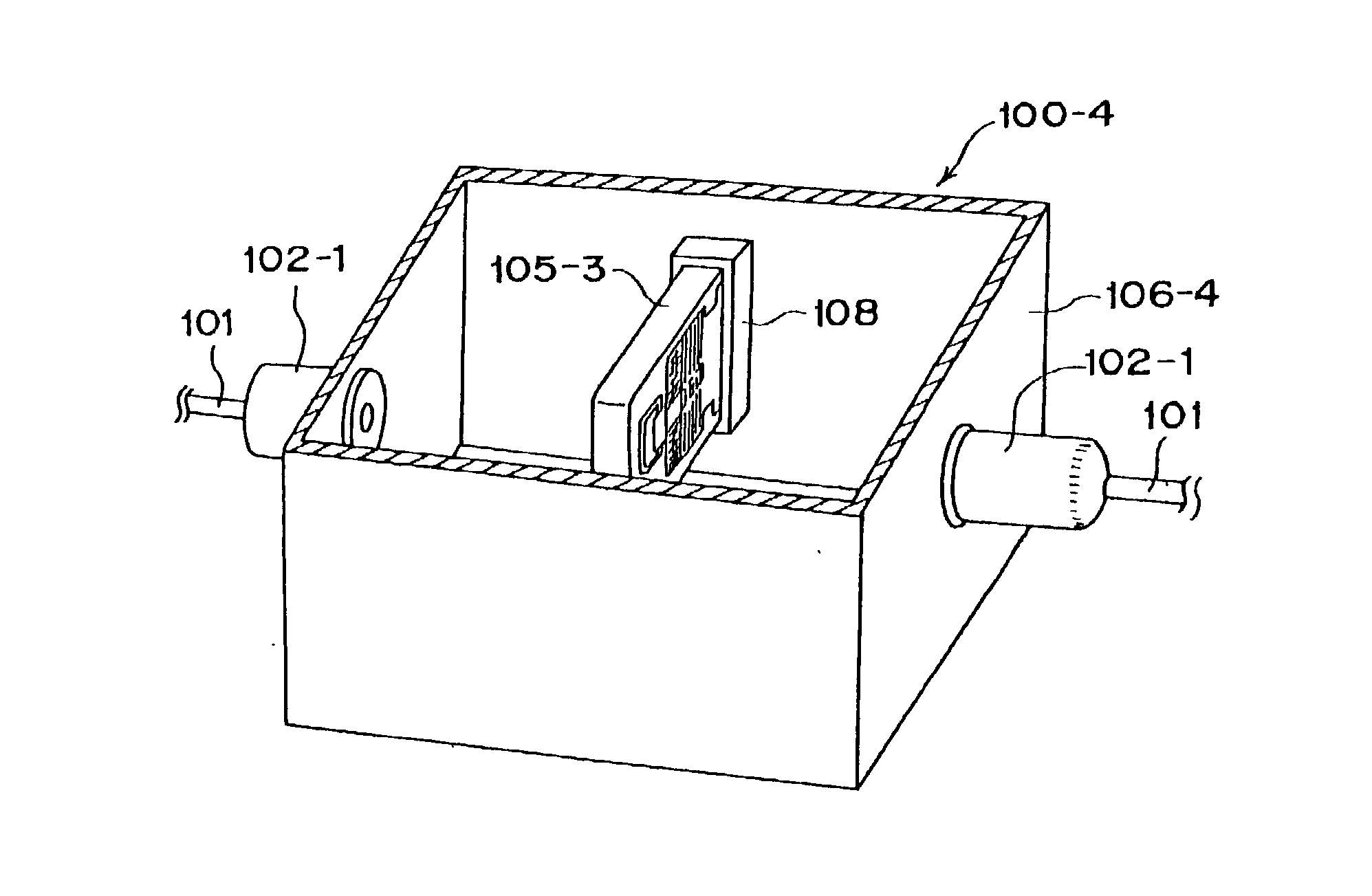
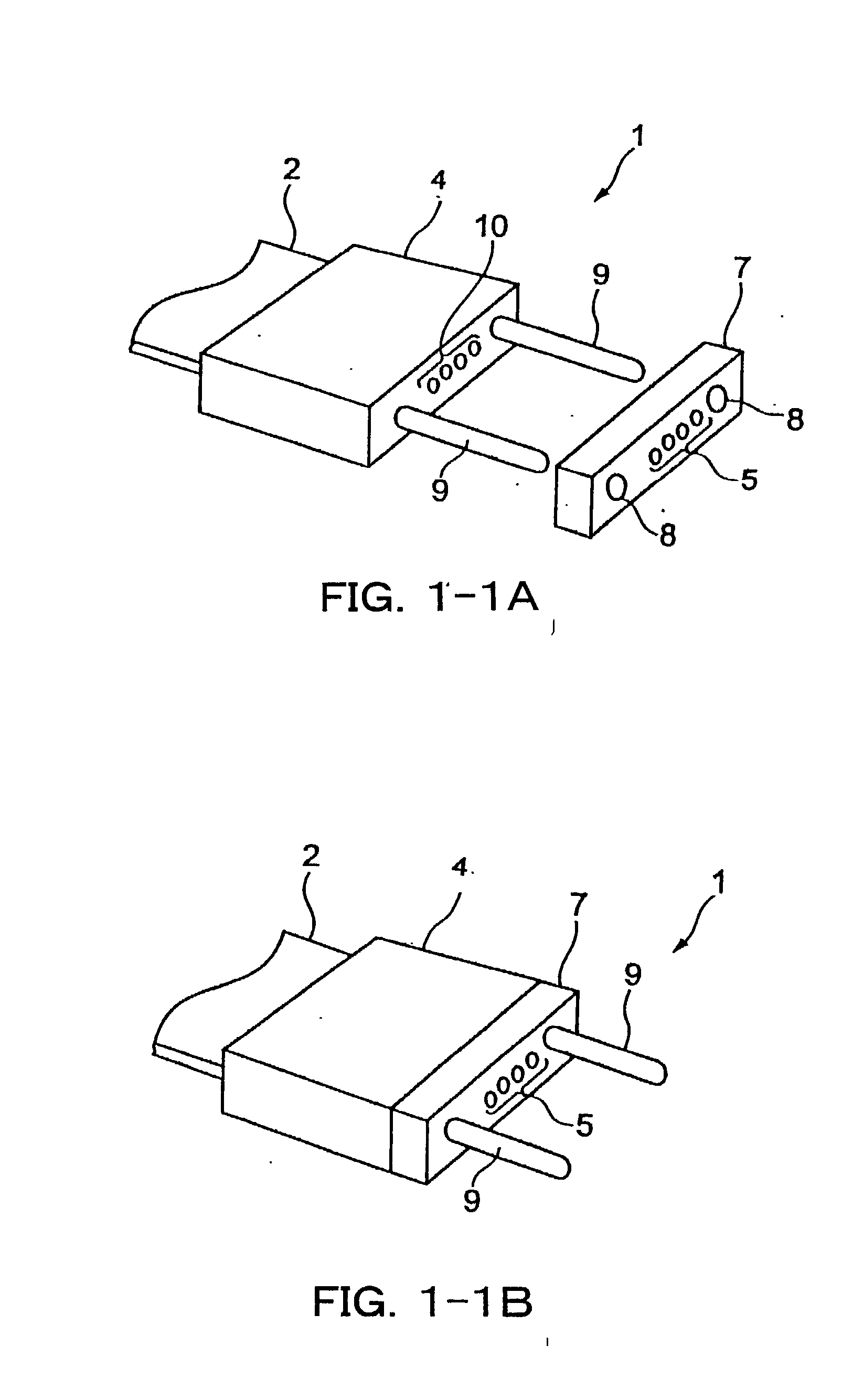
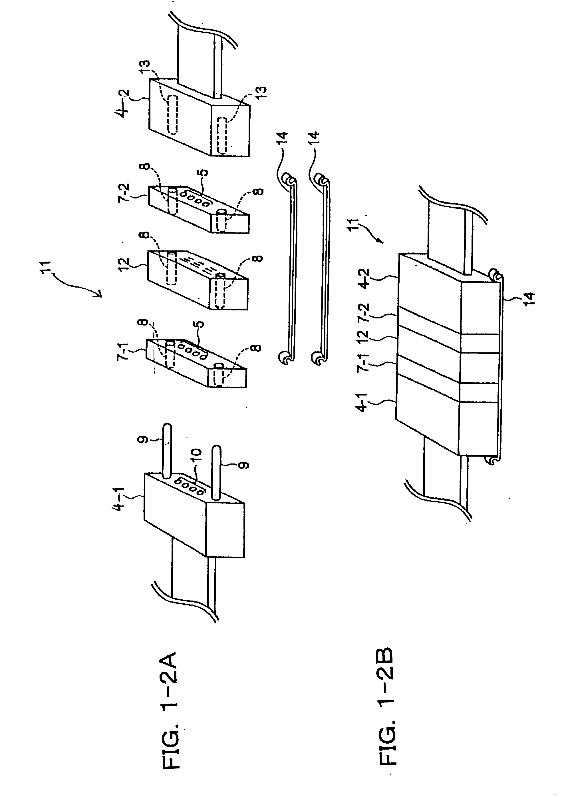
[0001] The first invention relates to a functional optical module having a ferrule that holds an optical fiber used in optical communications or the like, a collimator provided in contact with the ferrule, and an optical functional component that exerts a predetermined effect on a collimated light beam.[0002] The second invention relates to a power supply device for an optical functional component that exerts a predetermined effect on a light beam, and an optical functional module provided with the power supply device.[0003] The third invention relates to an optical switch used in, for example, optical path switching in an optical communication field.DESCRIPTION OF THE INVENTION[0004] (First Invention)[0005] FIG. 1-11 is a schematic view of a conventional functional optical module 100. In addition, the functional optical module 100 is provided with a variable optical attenuator as an optical functional component, but to facilitate explanations, only an optical absorptive filter 101 ...
Claims
Login to View More Application Information
Patent Timeline
 Patent Type & Authority Applications(United States)
IPC IPC(8): G02B6/26G02B6/32G02B6/35G02B6/38G02B6/42
CPCG02B6/264G02B6/266G02B6/32G02B6/352G02B6/353G02B6/357G02B6/4292G02B6/3594G02B6/3849G02B6/3885G02B6/3893G02B6/4201G02B6/4249G02B6/3574
Inventor MORIMOTO, MASAHITOSATO, KOUKISHIINO, MASATOKAZAMI, HAJIME
Owner FURUKAWA ELECTRIC CO LTD


