
Thin film memory, array, and operation method and manufacture method therefor

a film memory and array technology, applied in the field of thin film memory, can solve problems such as difficulty in assembling a large array

Inactive Publication Date: 2003-11-20
HAYASHI YUTAKA +3
View PDF3 Cites 29 Cited by
  • Summary
  • Abstract
  • Description
  • Claims
  • Application Information

AI Technical Summary

Benefits of technology

[0013] The present invention has been made in view of the above, and an object of the present invention is therefore to provide a capacitor-less SOI or other semiconductor thin film memory cell and memory cell array which are applicable to FDSOI. Another object of the present invention is to provide an SOI or other semiconductor thin film memory cell and memory cell array in which data is written or erased without using carrier multiplication in a drain high electric field portion, as well as an operation method and manufacture method for the memory cell and array.

Problems solved by technology

This leads to erroneous, albeit mild, writing called write disturb and thereforemakes it difficult to assemble a large array in which a large number of cells are connected to each bit line.

Method used


Image

  • Thin film memory, array, and operation method and manufacture method therefor
  • Thin film memory, array, and operation method and manufacture method therefor
  • Thin film memory, array, and operation method and manufacture method therefor

Examples


embodiment 1

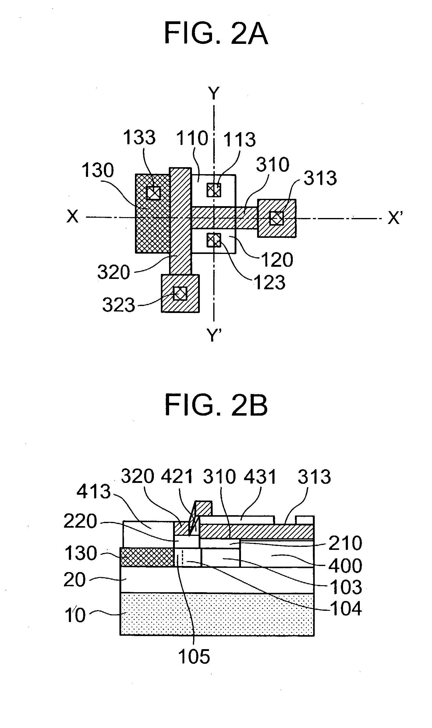
[0101] In Embodiment 1, cells of the present invention in FIGS. 5A and 5B are connected as shown in an equivalent circuit diagram of FIG. 7 to obtain a memory array. The memory array is operated by combination of voltages shown in Table 1 below. This array is suitable as a memory for a specific use because data can be written in cells of a word while data is read from cells of another word. The array is also suited for high speed refreshing operation. Table 1 shows the voltage relation among the word line, the writing bit line, the reading bit line, and the common line when the array is operated by a unipolar power supply of 1.2 V. Operation on a unipolar power supply is made possible by biasing the common line at a positive electric potential, usually, 0.5 V.

1TABLE 1 Operation Voltage Example of a Memory Array according to Embodiment 1 of the Present Invention Non-selected cell voltage (V) Selected cell voltage (V) Writing Erasing Reading Writing Erasing Reading Keeping CW CB CW CB...

embodiment 2

3TABLE 3 Operation Voltage Example of a Memory Array of the Present Invention Selected cell voltage (V) Non-selected cell voltage (V) Writing Writing (CW) Writing (CB) Reading "1" "0" Reading Keeping "1" "0" "1" "0" CW CB Keeping Word line 0 0 1.0 (first) 0.3 0 0 0.3 0.3 1.0 0.3 0.3 Bit line 0.6 0 0.5 0.3 0.3 0.3 0.6 0 0.3 0.5 0.3 Common line 0.3 0.3 0.3 0.3 0.3 0.3 0.3 0.3 0.3 0.3 0.3 CW (common word): cells sharing a word line CB (common bit): cells sharing a bit line

[0112] The word line voltage upon reading is supplied before the bit line voltage.

[0113] An acceptable change in voltage of one line is within .+-.0.1 V when the voltage of another line has the standard value. If the voltage of every line is changed in the same direction, the acceptable electric potential change is larger.

[0114] It is sufficient if the difference between the electric potential of each line and the electric potential of the common line satisfies the relation shown in Table 3. Accordingly, it may also ...


PUM


Abstract

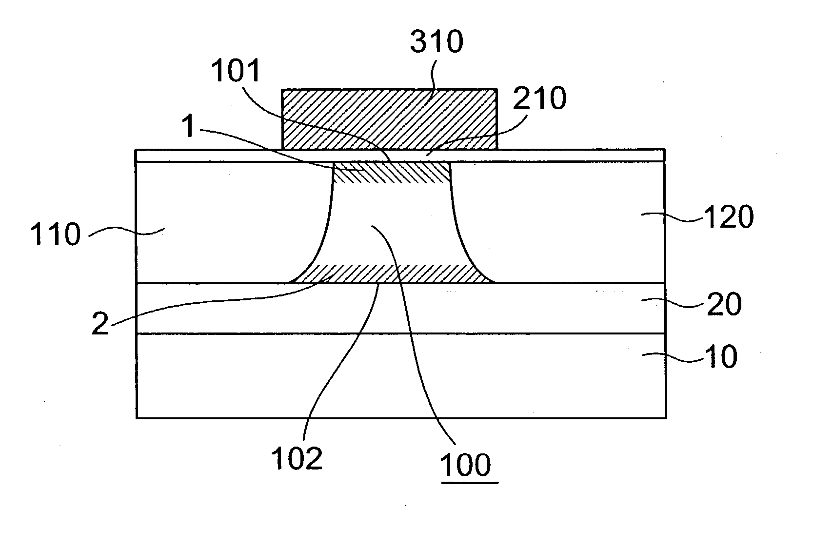
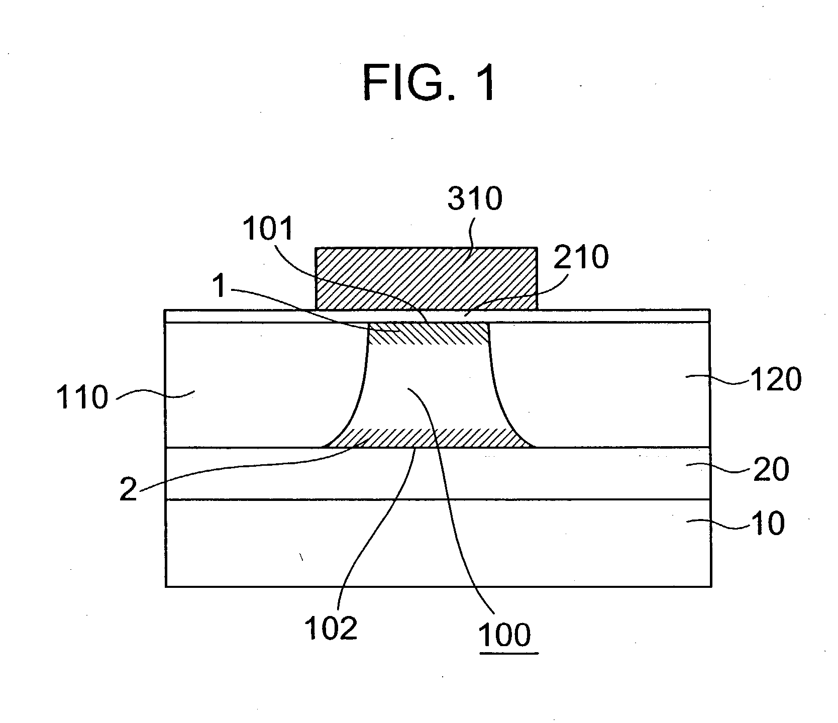
A memory cell which is formed on a fully depleted SOI or other semiconductor thin film and which operates at low voltage without needing a conventional large capacitor is provided as well as a memory cell array. The semiconductor thin film is sandwiched between first and second semiconductor regions which face each other across the semiconductor thin film and which have a first conductivity type. A third semiconductor region having the opposite conductivity type is provided in an extended portion of the semiconductor thin film. From the third semiconductor region, carriers of the opposite conductivity type are supplied to and accumulated in the semiconductor thin film portion to change the gate threshold voltage of a first conductivity type channel that is induced by a first conductive gate voltage in the semiconductor thin film between the first and second semiconductor regions through an insulating film.

Description

[0001] 1. Field of the Invention[0002] The present invention relates to a semiconductor memory and an integrated circuit built therefrom, and more specifically, to a technique which uses for a channel formation region a semiconductor thin film such as SOI (Semiconductor On Insulator) or SON (Semiconductor On Nothing). The semiconductor thin film is formed on an insulating substrate (SOI) in some cases, is suspended and held at both ends by substrates in a hollow state (SON) in some other cases, and has a projecting portion which is connected at one end to a substrate in still other cases.[0003] 2. Description of the Related Art[0004] H. J. Wann et al. have proposed in 1993 to obtain a dynamic memory that does not use a capacitor by incorporating two complementary transistors in a partially depleted SOIMOS transistor structure (See Non-patent Document 1, for example).[0005] Recently, a memory has been proposed in which carriers are generated utilizing a carrier multiplication phenome...

Claims


Application Information

Patent Timeline
Patent Type & Authority Applications(United States)
IPC IPC(8): H01L21/8242G11C16/04H01L27/108
CPCH01L21/84H01L27/10802Y10S257/908H01L27/1203H01L27/10844H10B12/20H10B12/01H01L21/18
Inventor HAYASHI, YUTAKAHASEGAWA, HISASHIYOSHIDA, YOSHIFUMIOSANAI, JUN
Owner HAYASHI YUTAKA
Learn More