
Eureka
For R&D, Eureka makes reading and utilizing patents & technical documents easy.
Eureka AIR
Designed for self-driven R&D workflows. Generate viable solutions, solve complex R&D challenges, empower your innovation with AI.

Eureka Materials
Designed for material experts only. Revolutionize your material R&D, from search, analyze, to developing new materials.

TechResearch
Generate reliable direction feasibility study reports for your R&D in just a few steps.

TechSeek
Discover and master advanced knowledge NOW. Basics, ideas, possibilities, all at once.

TechMind
As an expert in R&D Theories, TechMind can generates customized viable solutions instantly.

TechRisk
Analyze your overall solution with one click, know your potential R&D risks in advance.

TechMonitor
Get weekly tech updates, stay abreast of the latest tech innovations and key insights.
Selection of wavelengths for integrated circuit optical metrology
- Summary
- Abstract
- Description
- Claims
- Application Information
AI Technical Summary
Benefits of technology
Problems solved by technology
Method used
Image

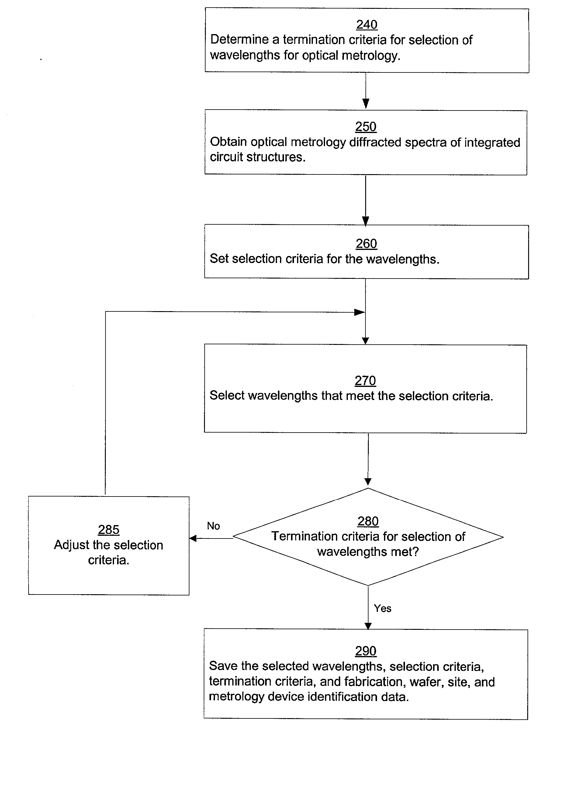
Examples
Embodiment Construction
)
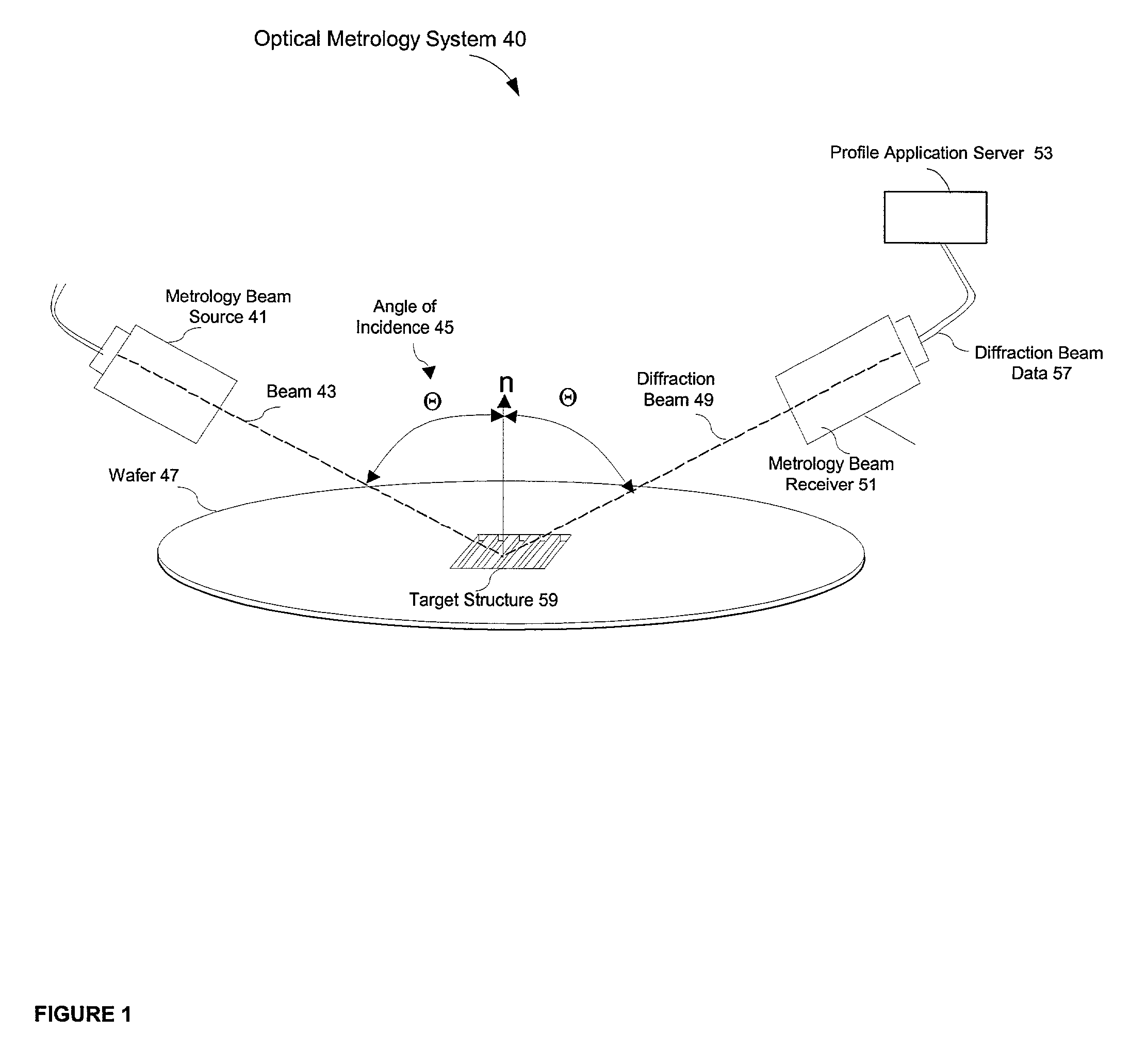
[0028] In order to facilitate the description of the present invention, an ellipsometric optical metrology system is used to illustrate the concepts and principles. It is understood that the same concepts and principles equally apply to the other IC optical metrology systems such as reflectometric systems and the like. In a similar manner, although a diffraction spectra and profile library is frequently used to illustrate concepts and principles, the present invention equally applies to a data space comprising profile parameters and corresponding metrology signals.
[0029] FIG. 1 is an architectural diagram illustrating the use of optical metrology to measure the diffraction signals off integrated circuit structures. The optical metrology system 40 includes a metrology beam source 41 projecting a beam 43 at the target structure 59 of a wafer 47. The metrology beam 43 is projected at an incidence angle .theta. towards the target structure 59. The diffraction beam 49 is measured by a m...
PUM
 Abstract
Description
Claims
Application Information
 - R&D Engineer
- R&D Manager
- IP Professional
- Industry Leading Data Capabilities
- Powerful AI technology
- Patent DNA Extraction
Browse by: Latest US Patents, China's latest patents, Technical Efficacy Thesaurus, Application Domain, Technology Topic, Popular Technical Reports.
© 2024 PatSnap. All rights reserved.Legal|Privacy policy|Modern Slavery Act Transparency Statement|Sitemap|About US| Contact US: help@patsnap.com