Dual damascene semiconductor devices

a semiconductor device and damascene technology, applied in semiconductor devices, semiconductor/solid-state device details, electrical devices, etc., can solve the problems of reducing the delay component, and increasing the complexity of wiring circuitry

a semiconductor device and damascene technology, applied in semiconductor devices, semiconductor/solid-state device details, electrical devices, etc., can solve the problems of reducing the delay component, and increasing the complexity of wiring circuitry

US20030227090A1Inactive Publication Date: 2003-12-11SHARP KK

Image

  • Dual damascene semiconductor devices
  • Dual damascene semiconductor devices
  • Dual damascene semiconductor devices

Examples


Embodiment Construction

(PMA) photocrosslinking polymer Comparative Polymethylmethacrylate No 180 Example 2 (PMMA) photodegradable polymer

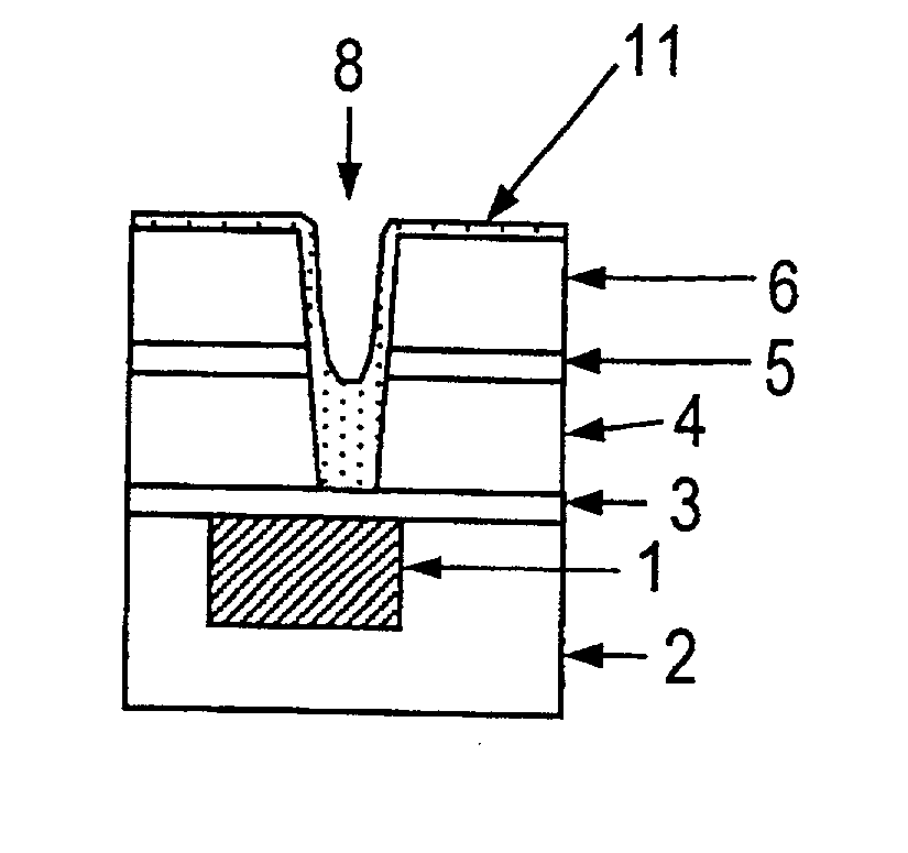
[0046] While an excimer lamp with a 172 nm wavelength is used in the radiation processing in this example of application, another method may be used if it is a radiation source that can cause a break in the main chain of polymer 11. For example, an electron beam, ArF excimer laser light, an F.sub.2 excimer laser light or soft X-rays may be used.

[0047] Likewise, an amount of such materials as carbon or fluorine may be mixed in with the silicon oxide film 4 or 6. In addition, the nitrided silicon film 5 may also be dispensed with.

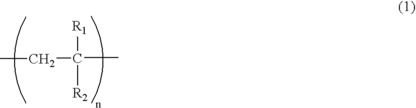
[0048] Although polymethylmethacrylate (PMMA) is used for the polymer film 11 in this example, any polymeric material or mixture that decomposes upon exposure to radiation can be used. These polymeric materials include polyisobutylene, poly-.alpha.-methylstyrene, polyacrylate, polymethacrylate, polymethacrylamide, polyvinylidene chloride, cellulos...


PUM


Abstract

A semiconductor device has a wiring slot and two wiring layers connected by a via hole. The semiconductor device is formed using a photodegradable polymer film that degrades under UV radiation. An incidence angle theta of radiation rays in the irradiating step with respect to a perpendicular direction of a surface of the substrate, fulfills the relationship tan theta>=H+H' / 2(D+D') wherein D is a depth of the wiring slot, D' is a thickness of the photoresist film, H is a diameter of the via hole in a opening of the wiring slot, and H' is the width of the wiring slot.

Description

[0001] This invention is directed semiconductors having wiring components with dual damascene structures in the upper part of a first wiring layer.BACKGROUND OF INVENTION[0002] With each succeeding generation, semiconductor integrated circuits increase in speed and their features proliferate. Two factors govern the speed of signal transmission in semiconductor circuits: 1) switching time (gate delay component) in the transistor portion, and 2) the time that an electrical signal is propagated in a circuit (wiring delay component). The gate delay component tends to decrease with the reduction of transistor size, while the wiring delay component tends to increase with the refinement, i.e., diminuation, in size of wiring layers and the increasing complexity of wiring circuitry. Since wiring delay is determined by the product (C.times.R) of wiring capacity C and wiring resistance R, the use of Cu as a material for wiring has been enthusiastically studied as a means of restricting wiring ...

Claims


Application Information

Patent Timeline
11 Dec 2003
Publication
US20030227090A1
IPC
H01L21/768; H01L23/532
CPC
H01L21/76808; H01L23/53295; H01L2924/12044; H01L2924/0002; H01L2924/00
Inventors
OKABE, ICHIRO