Subpad having robust, sealed edges

a subpad and robust technology, applied in flexible wheel, chemistry apparatus and processes, manufacturing tools, etc., can solve the problems of circuitry size, the design size of such integrated chips is steadily decreasing, and the production of ever smaller and increasingly complex microcircuits

Active Publication Date: 2003-12-11
ROHM & HAAS ELECTRONICS MATERIALS CMP HLDG INC
View PDF11 Cites 24 Cited by
  • Summary
  • Abstract
  • Description
  • Claims
  • Application Information

AI Technical Summary

Benefits of technology

[0013] An object of the present invention is to provide a belt or pad with treated edges that prevents slurry or liquids from entering the edges of the subpad of the belt or pad.
[0014] An object of the present invention is to provide a belt and pad with an improved seal between the edges of the subpad and the polishing layer so as to prevent slurry or liquids from coming into contact with the edges of the subpad. It is a further object of the invention to provide an improved seal between the edges of the subpad and the polishing layer that is able to maintain its integrity during extreme temperatures, pressures and stresses.
[0015] An object of the invention is to provide a polishing belt or pad with robust sealing of the edges of the subpad so as to prevent a slurry from penetrating said subpad.

Problems solved by technology

The designed size of such integrated chips is steadily decreasing, while the number of layers applied, e.g. by lithography onto the silicon surface, is rising to produce ever smaller and increasingly complex microcircuits.
The decrease in the size of circuitry and the increase in the number of layers applied are leading to ever more stringent requirements on the smoothness and planarity of the silicon and semiconductor wafers throughout the chip manufacturing process, since uneven surfaces ultimately result in imperfections and defects leading to unplanned resistances where a conductor is narrowed, to capacitances / nonconductive gaps where breaks occur in deposited conductor layers, and to unplanned short circuits where insulating barriers are breached, which interfere with or compromise the planned operation of the circuit.
And when liquid (e.g., the CMP slurry) soaks into the subpad, the subpad's physical properties change, which in turn changes or impairs the polishing performance of the polishing layer stacked onto the subpad.
Those strategies, while helpful, are not without their disadvantages and drawbacks.
One significant drawback is that the seals and / or adhesives used in these strategies are exposed to attack by the CMP slurry, which can degrade the seals and / or delaminate the polishing layers.
Another disadvantage is that the belt or pad user must perform the sealing operation at the site of use, rather than having the belt manufacturer preseal the subpad edges.
Finally, the edge sealing of the prior art is unsuitable for continuous polishing belts which subject the edge seals to pronounced stretching and bending forces as the belt is pulled around the spinning rollers.
The excessive bending and stretching compounded with the high stresses and rotational speed of the belts often lead to cracks and fractures in the edge sealant through which the CMP slurry may enter the subpad.

Method used


Image

  • Subpad having robust, sealed edges
  • Subpad having robust, sealed edges
  • Subpad having robust, sealed edges

Examples


Embodiment Construction

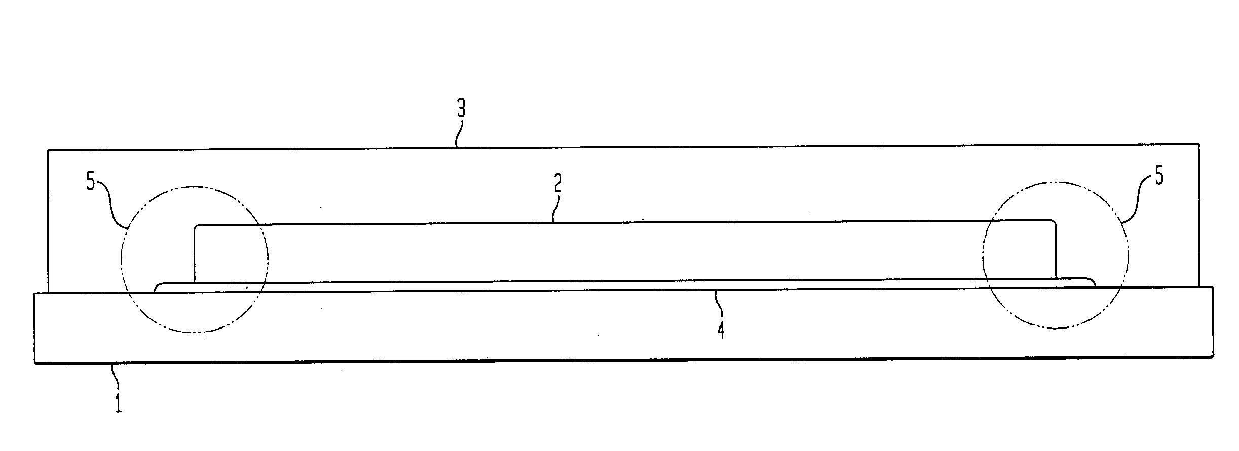
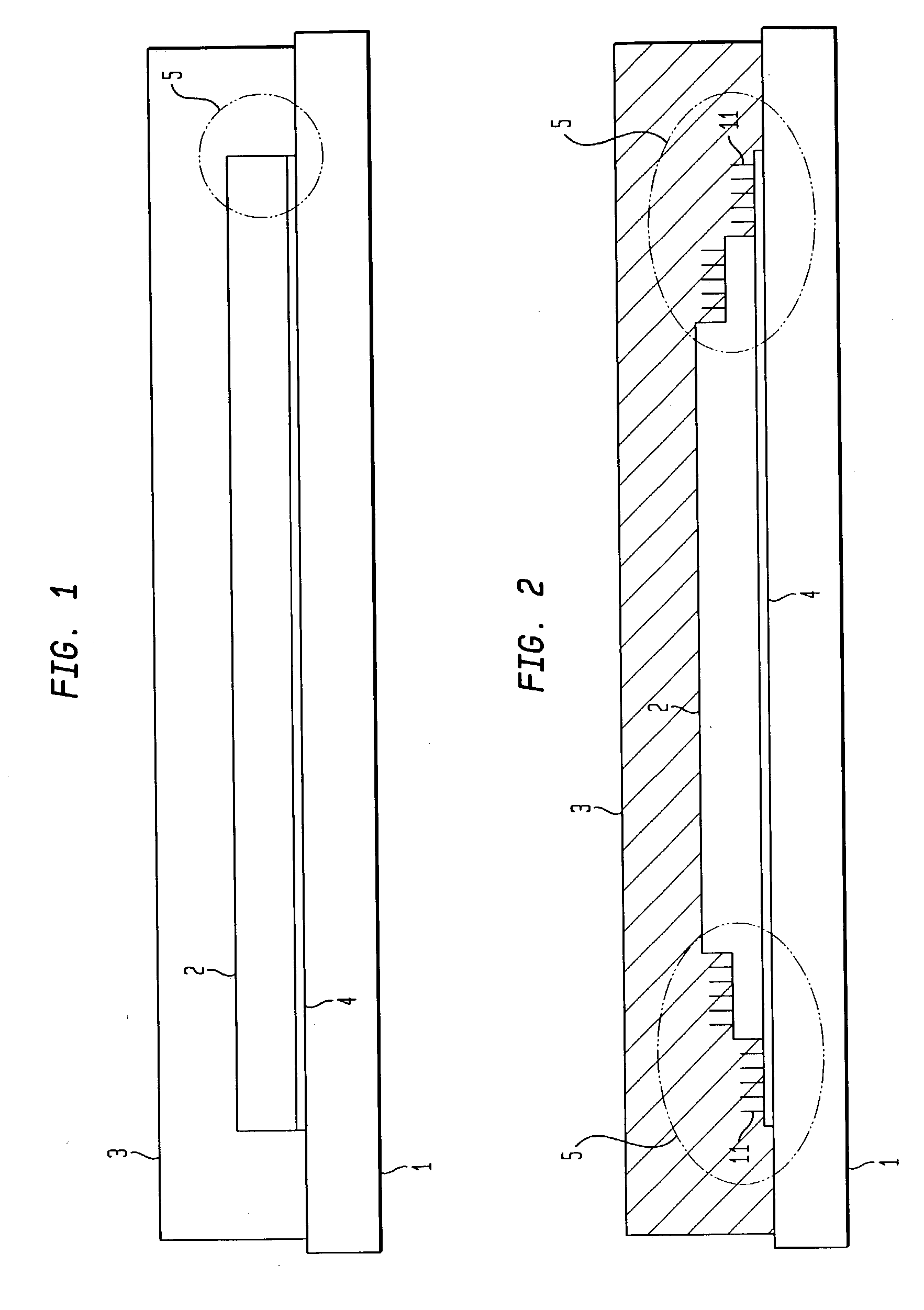
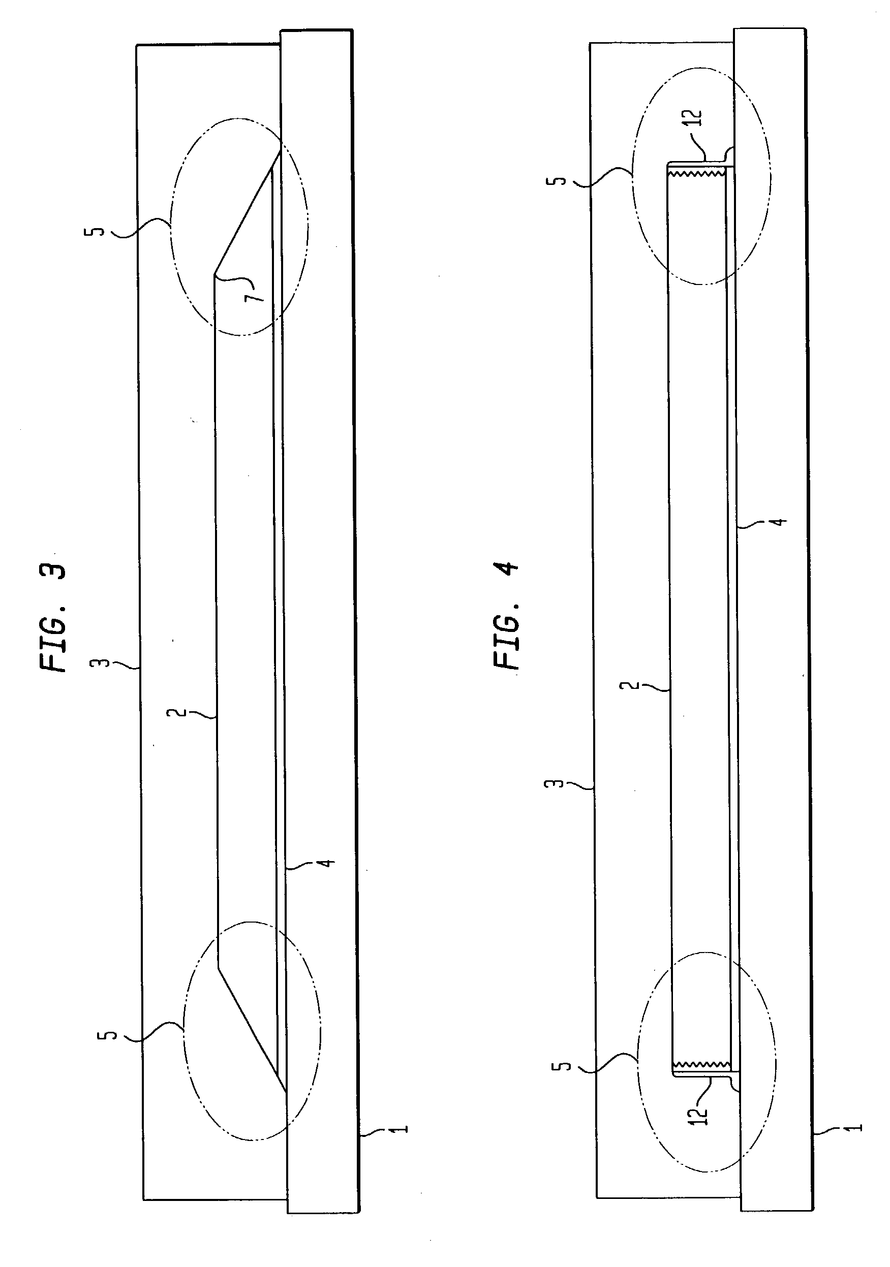
[0037] The pads according to this invention can be used to polish any type of material or layer in any of various polishing steps, such as, for example, in semiconductor manufacturing. Typical materials to be polished include but are not limited to silicon, silicon dioxide, copper, tungsten, and aluminum. The polishing pad may be designed to selectively polish some materials and not others, to polish dissimilar materials at similar rates, or to work specifically with certain specific types of slurries and solutions. Although the pads of the present invention are especially suited for the chemical-mechanical polishing of electronic workpieces, such as silicon and semiconductor wafers, hard discs etc, the pads and belts of the present invention may also be used to polish other substrates, for example for polishing and planarizing optical flats and mirrors. In addition, the pad of the present may be applicable in other industries such as the pharmaceutical, chemical, and food industrie...


PUM


Abstract

Provided are encapsulated belts and encapsulated pads for use in a variety of polishing application, including the chemical-mechanical polishing and planarization of semiconductor wafers and other workpieces. The encapsulated belts and pads are characterized by a robust seal between a polishing layer of the pad or belt and the edges of the subpad layer of the pad or belt. The robust seal is accomplished by casting a polymer directly over the subpad layer. The edges of the subpad layer may include one or more functional features that promote the formation of a watertight and slurry-resistant seal when the subpad layer is covered with a cast polymer. Also provided is a method of producing a robust seal between the polishing layer and the edge region of the subpad by encapsulating a subpad layer with a polymeric material.

Description

[0001] This application claims priority to U.S. Provisional Application No. 60 / 386,943, filed Jun. 7, 2002.[0002] 1. Field of the Invention[0003] The present invention relates to improved sealing of subpad edges used for a variety of applications, including semiconductor polishing.[0004] 2. BACKGROUND OF THE INVENTION[0005] Silicon wafers are produced as precursors from which microelectronic semiconductor components are produced. The wafers are cut from cylindrical silicon crystals, parallel to their major surfaces, to produce thin disks, typically 20-30 cm in diameter, although larger or smaller wafers are possible. The resulting wafers must be polished to give flat and planar surfaces for deposition of electronic components onto the surface by standard lithographic and etching techniques to form integrated chip semiconductor devices. Typically a 20-cm diameter wafer will produce about 100 or more microprocessor chips.[0006] The designed size of such integrated chips is steadily de...

Claims


Application Information

Patent Timeline
Patent Type & Authority Applications(United States)
IPC IPC(8): B24B37/22B24B37/24B24D13/14H01L21/321
CPCB24B37/22H01L21/3212B24B37/24B32B37/26
Inventor LOMBARDO, BRIANCIANCIOLO, JOSEPH
Owner ROHM & HAAS ELECTRONICS MATERIALS CMP HLDG INC
Why Eureka
Try Eureka