
Conveyance system, conveyance method and vacuum holding apparatus for object to be processed, and centering method for water

Inactive Publication Date: 2004-03-11
TOKYO ELECTRON LTD
View PDF7 Cites 19 Cited by
  • Summary
  • Abstract
  • Description
  • Claims
  • Application Information

AI Technical Summary

Benefits of technology

[0010] In order to solve the above-mentioned problem, an object of the present invention is to provide a conveyance method for objects to be processed and a semiconductor manufacturing device for the objects, both of which enable loading of the objects in spite of a single load port as if the semiconductor manufacturing device had a plurality of load ports, without requiring an excessive space, thereby preventing the footprint and the manufacturing cost from increasing. Additionally, another object of the present invention is to provide a centering device that can center an object to be processed certainly when transferring objects to be processed, one by one.
[0015] In order to solve the above-mentioned problems, an object of the present invention is to provide a centering method for wafers, which eliminates a process exclusive to the centering operation and the optical sensor for centering thereby enabling contribution to an improvement in the throughput and a reduction in the device cost.
[0020] In order to solve the above-mentioned problem, an object of the present invention is to provide a vacuum holding device for objects to be processed, which can assure a sufficient flow rate of exhaust gas in spite of a low-capacity battery on board of a moving body, thereby allowing the object to be absorbed in vacuum certainly.

Problems solved by technology

However, if a wafer to be inspected has a large diameter of, for example, 300 mm, it becomes almost impossible for an operator to handle a carrier having a plurality of such wafers because the carrier is remarkably heavy.
Even if the operator can handle the carrier, the operator's carrying alone may be accompanied with a risk.
Further, since the management about particles in a clean room has become severe with the hyperfineness of semiconductor devices, the automatization of manufacturing installations, such as carrier conveyer, is taking on importance increasingly in view of managing particles in the clean room.
Additionally, due to the large-diameter and hyperfineness of a wafer, there is a jump in the number of devices to be formed in a single wafer, requiring a long period for completing a process, such as inspection, for one wafer.
Moreover, to process wafers in lot unit would cause the wafers after processing to stay in a prober until the processing operation will be completed in all of the wafers in the lot, thereby delaying a time for feeding the wafers in lot unit to a sequent process.
Consequently, it becomes difficult to shorten TAT (Turn-Around-Time) in the production.
On the other hand, since there is a recent tendency that the carrier becomes heavy for the wafers having large diameters thereby making it difficult and risky for an operator to handle such a carrier, Japanese Patent Publication (kokai) No. 10-303270 proposes a conveyance method that employs an automated guided vehicle (which will be referred as "AGV" after) to transport the carrier thereby to allow wafers in the same lot to be delivered between the vehicle and an process installation, in carrier unit.
However, if one carrier is present in the semiconductor manufacturing device having the only load port, the next carrier cannot be loaded unless the previous carrier is unloaded from the semiconductor device as a result of completion of processing all the objects in this carrier.
Thus, the operation for processing the objects comes to a standstill during loading and unloading the carrier, so that an improvement in the throughput of the system cannot be expected.
While, if establishing new load ports in the semiconductor device, then a problem arises in the increase in footprint and also manufacturing cost.
Furthermore, in the situation such that the carrier becomes heavy for the wafers having large diameters thereby making it difficult and risky for an operator to handle such a carrier, Japanese Patent Publication (kokai) No. 10-303270 proposes the conveyance method that employs the automated guided vehicle (which will be referred as "AGV" after) to transport the carrier thereby to allow wafers in the same lot to be delivered between the vehicle and an process installation, in carrier unit.
However, due to the large-diameter and hyperfineness of a wafer, there is a jump in the number of devices to be formed in a single wafer, requiring a long period for completing various processing, such as inspection, for one single wafer.
Therefore, even if the wafers in the same lot could be transported to a semiconductor manufacturing device, such as inspecting device, in carrier unit by the AGV, the processing of wafers in lot unit would require considerable date and time while causing even the wafers after processing to stay in the semiconductor manufacturing device.
Consequently, the time to feed the wafers in lot unit to a sequent process is delayed to that extent, so that it becomes difficult to shorten TAT (Turn-Around-Time) in the production.
Therefore, there are problems that it takes a lot of time for centering a wafer and a lot of cost for the optical sensor for this centering.
Further, if a wafer to be inspected has a large diameter of, for example, 300 mm, it becomes almost impossible for an operator to handle a carrier having a plurality of such wafers because the carrier is remarkably heavy.
Even if the operator can handle the carrier, the operator's carrying alone may be accompanied with a risk.
However, due to the large-diameter and hyperfineness of a wafer, there is a jump in the number of devices to be formed in a single wafer, requiring a long period for completing an inspection of one wafer.
Moreover, the inspection of wafers in lot unit would cause the wafers after inspecting to stay in a prober (carrier) until the inspection of all of the wafers in the lot is completed, thereby delaying a time for feeding the wafers in lot unit to a sequent process.
Consequently, it becomes difficult to shorten TAT (Turn-Around-Time) in the production.
However, since there exists a limitation in the power capacity of a battery forming a drive source for the compressor, on board of the AGV, it is impossible to assure a sufficient flow rate of exhaust gas necessary for the vacuum absorption.

Method used


Image

  • Conveyance system, conveyance method and vacuum holding apparatus for object to be processed, and centering method for water
  • Conveyance system, conveyance method and vacuum holding apparatus for object to be processed, and centering method for water
  • Conveyance system, conveyance method and vacuum holding apparatus for object to be processed, and centering method for water

Examples


Embodiment Construction

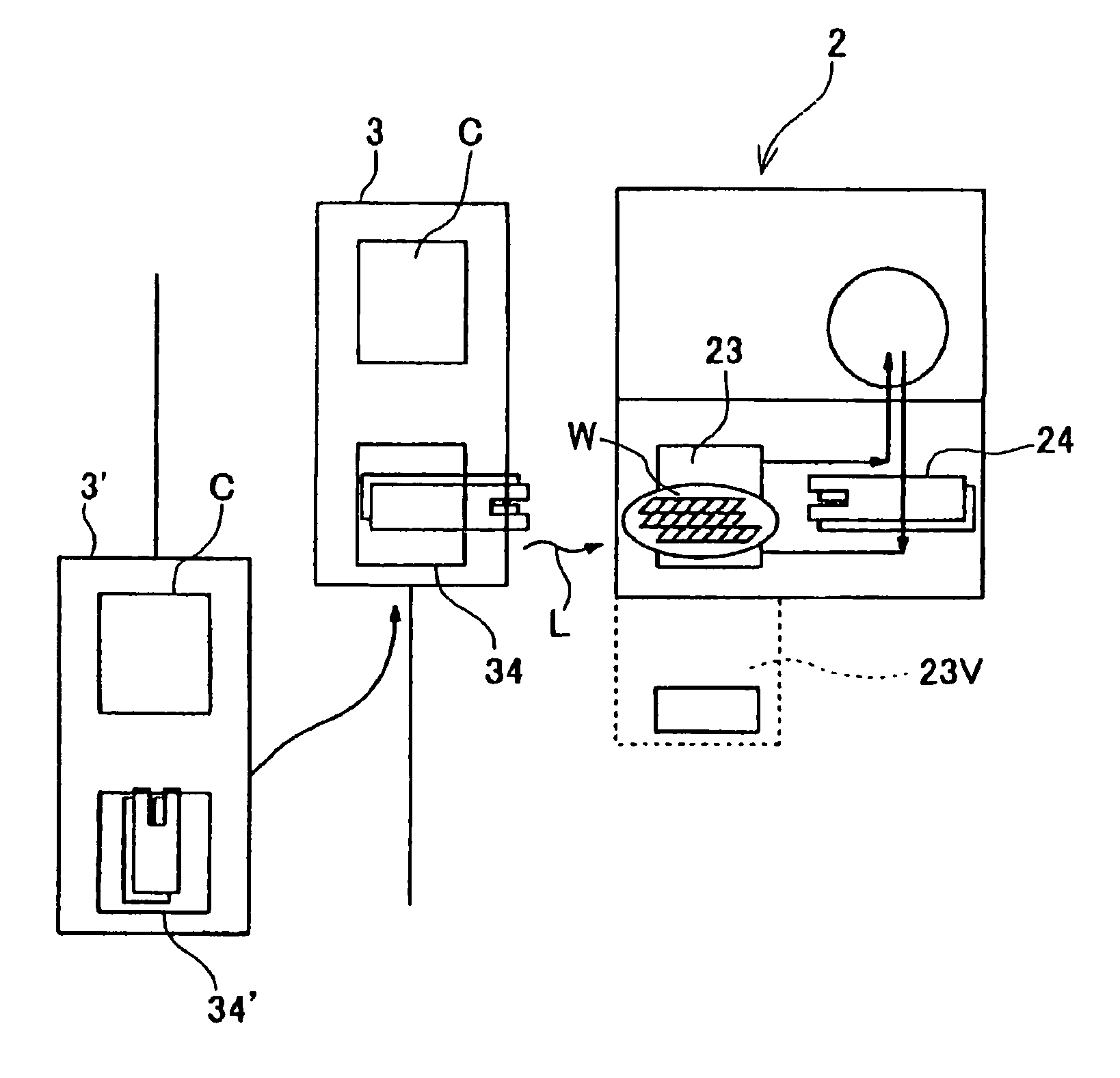
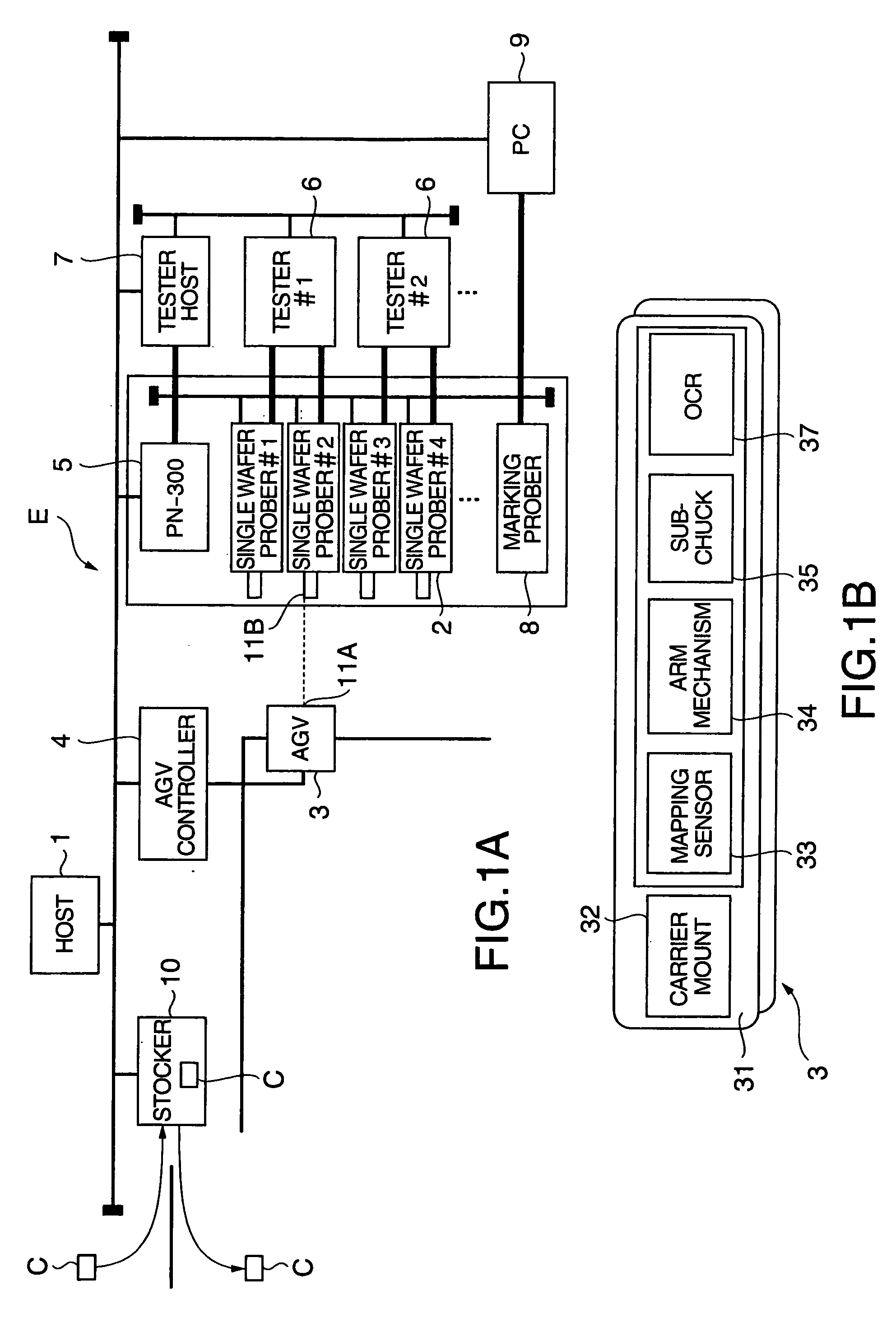
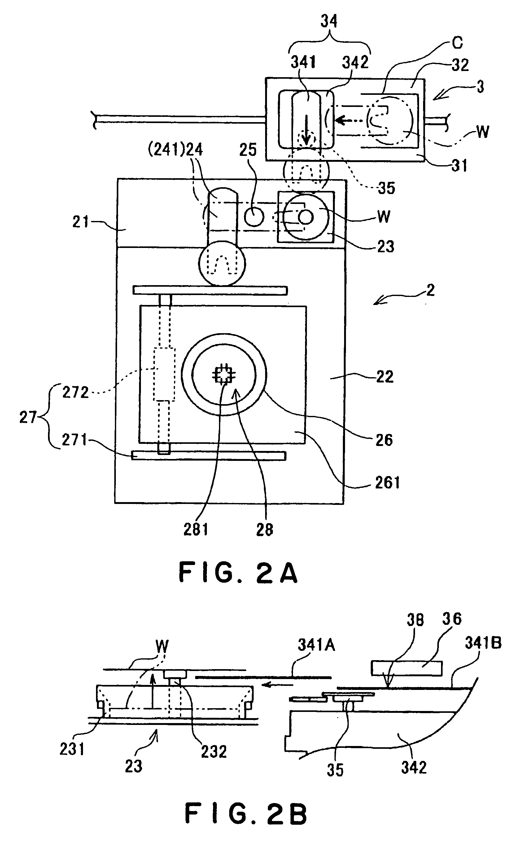
[0084] Based on embodiments shown in FIGS. 1A to 17B, the present invention will be described below.

[0085] First of all, we now describe a conveyance system for objects to be processed, which is employed in a conveyance method for the objects to be processed in accordance with the present invention. As shown in FIGS. 1A and 1B, the conveyance system (Automated material handling system (AMHS)) E includes a host computer for carrying out the product management of the whole factory including an inspection process for wafers (not shown) as the objects to be processed, a plurality of semiconductor manufacturing devices, for example, inspecting devices (e.g. probers) 2 for inspecting the electrical characteristics of the wafers under the administration of the host computer 1, a plurality of sheet-type automatic transporting devices (which will be called as "AGVs" after) 3 for automatically transporting the wafers one by one to these probers 2 according to respective demands and a transpor...


PUM


Abstract

A conveyance system E for wafers W includes a host computer 1 for carrying out the management of the production of semiconductor devices, a plurality of probers 2 for inspecting the electric characteristics of the wafers W under the administration of the host computer 1, an AGV 3 for automatically transporting the wafers W in block of a carrier in order to deliver the wafers W one by one to these probers 2 according to respective demands and an AGV controller 4 for controlling the operation of the AGV 3 under the administration of the host computer 1.

Description

[0001] The present invention relates to a conveyance system for an object to be processed and a conveyance method for the object to be processed. More in detail, the invention relates to conveyance system and method for the objects to be processed, that transport the objects to a semiconductor manufacturing device, such as inspecting device, in single wafer unit against the objects. Further, the present invention relates to a method for centering a semiconductor wafer in advance of processing the wafer.[0002] Further, the present invention relates to a vacuum holding apparatus, more in detail, the vacuum holding apparatus for an object to be processed, which is carried by a moving body, such as automatic transporting device.BACKGROUND OF ART[0003] In the inspection process of semiconductor devices, for example, a prober is widely used as an inspecting device for inspecting semiconductor wafers (the semiconductor waters will be simply referred "wafers", after.). Normally, the prober ...

Claims


Application Information

Patent Timeline
IPC IPC(8): G05B19/00G05B19/418H01L21/00H01L21/68
CPCG05B19/00G05B19/41815H01L21/6835G05B2219/45031H01L21/67276G05B2219/31002Y02P90/02Y02P90/60H01L21/6773H01L21/67769
Inventor AKIYAMA, SHUJIIIJIMA, TOSHIHIKOHOSAKA, HIROKI
Owner TOKYO ELECTRON LTD
Learn More