Method for removing resist pattern and method for manufacturing semiconductor device

a technology of resist pattern and manufacturing method, which is applied in the direction of photosensitive materials, instruments, photomechanical equipment, etc., can solve the problems of difficult to remove resist pattern after doping or dry etching, difficult to remove deteriorated layer over the surface, and difficult to remove resist pattern

Inactive Publication Date: 2004-05-13
SEMICON ENERGY LAB CO LTD
View PDF27 Cites 20 Cited by
  • Summary
  • Abstract
  • Description
  • Claims
  • Application Information

AI Technical Summary

Problems solved by technology

However, in the resist removing process, it is known that a resist pattern after doping or dry etching becomes difficult to remove.
For example, when a resist pattern over a substrate passes through a dry etching process, the reaction of polymers which constitute a resist pattern with an etching gas and the cross-linking reaction between the polymers proceed and a deteriorated layer difficult to remove is produced over the surface of the resist pattern.
The de

Method used


Image

  • Method for removing resist pattern and method for manufacturing semiconductor device
  • Method for removing resist pattern and method for manufacturing semiconductor device
  • Method for removing resist pattern and method for manufacturing semiconductor device

Examples


Embodiment Construction

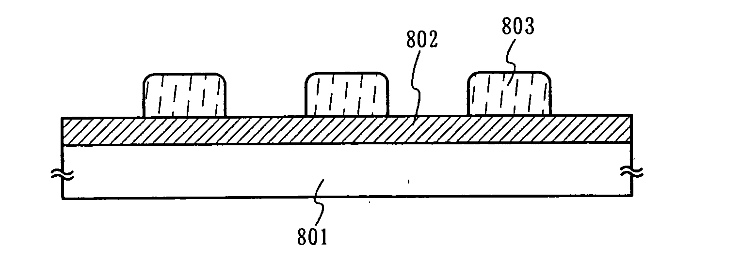
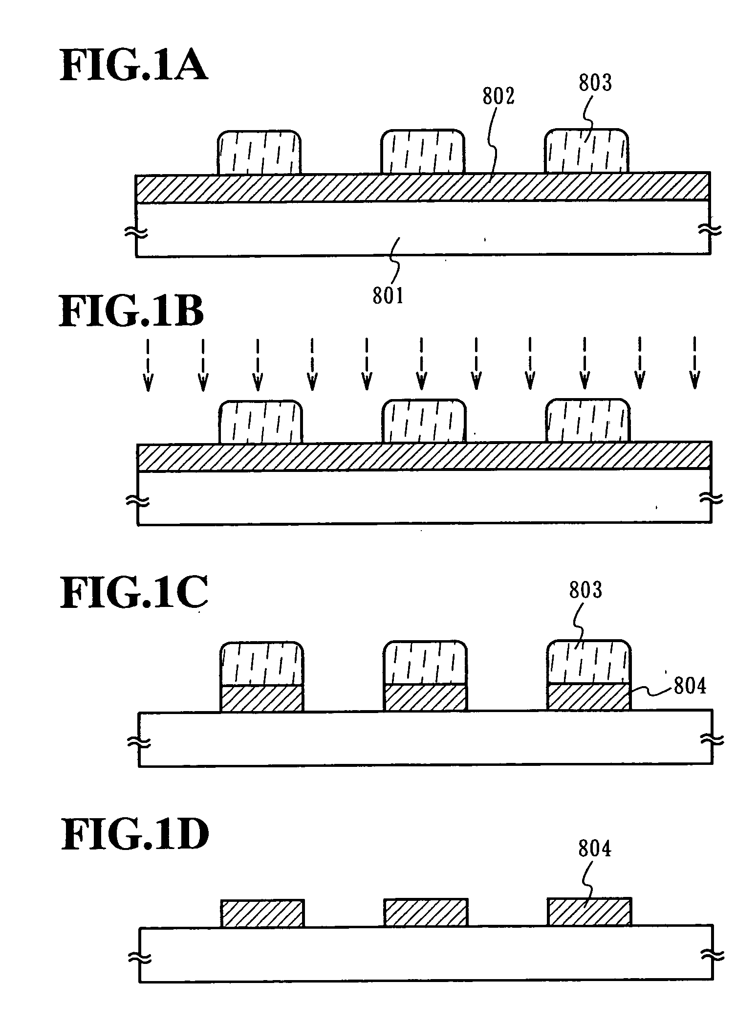
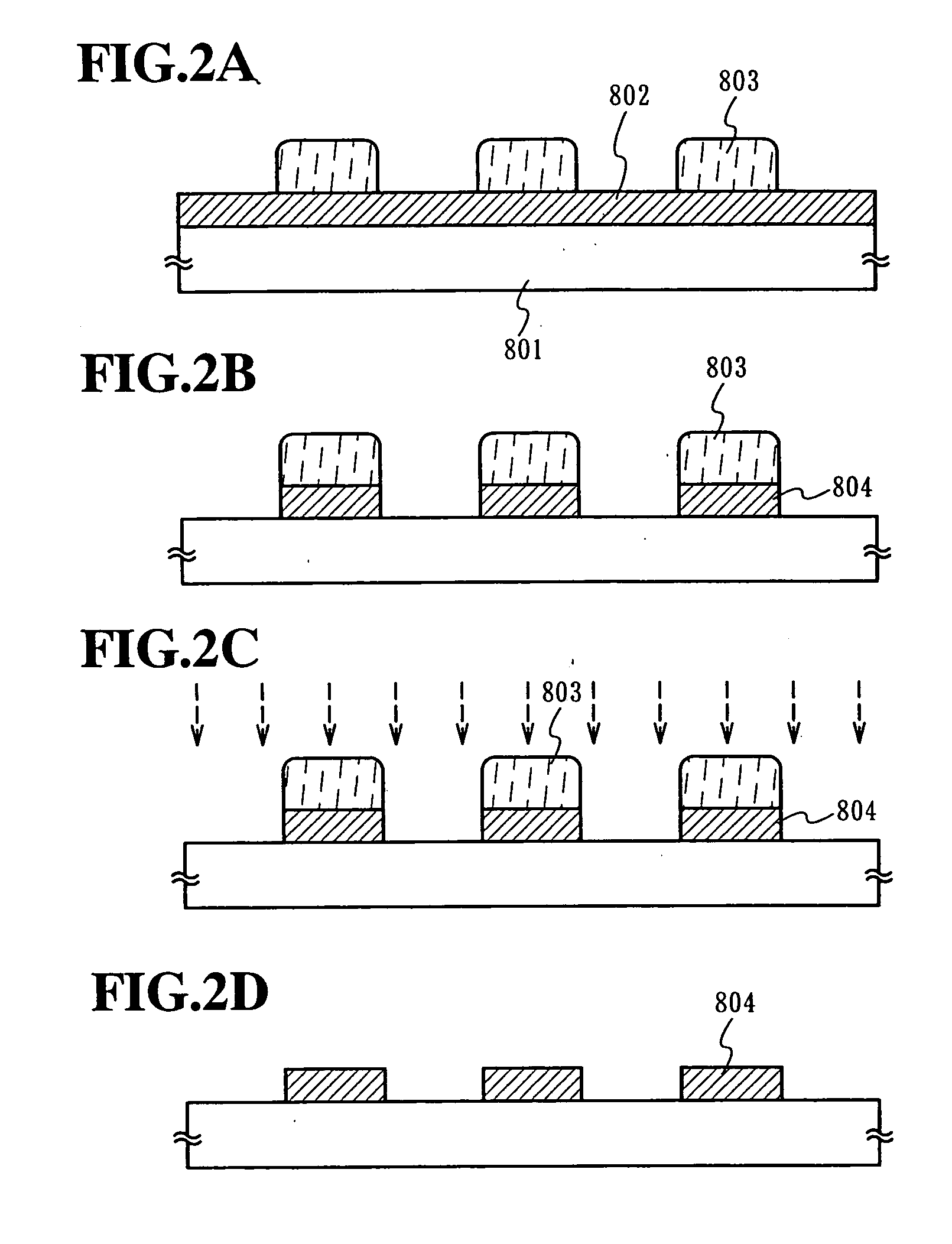
[0073] An acrylic resin layer having a thickness of 800 nm was formed on a glass substrate. A titanium nitride (TiN) film, an aluminum (Al:Si (1 wt %)) film, a titanium nitride (TiN) film, and a titanium (Ti) film were laminated in the stated order on the thus-formed acrylic resin layer in thicknesses of 60 nm, 40 nm, 300 nm, and 100 nm, respectively. Then, a diazonaphthoquinone (DNQ)-novolac resin type of positive resist composition was applied on the resultant laminate and subjected to a pre-baking treatment for a predetermined period of time at a treating temperature of about 100.degree. C. to form a resist film having a predetermined thickness. Thereafter, the thus-formed film was subjected to an exposure treatment for a predetermined period of time by using a 1:1 projection aligner utilizing light having a multiple of wavelengths (e.g., g-line, h-line, and i-line) of an ultra high-pressure mercury lamp and, then, subjected to a development treatment for a predetermined period o...


PUM


Abstract

It is an object to provide a technique for removing a resist favorably without leaving residue in the case of using a nonaqueous resist stripper. According to the present invention, in order to achieve the object, when a resist pattern is removed by using the nonaqueous resist stripper, it becomes easier to remove the resist pattern after dry etching or ion doping, by performing exposure treatment on the resist pattern. After a resist pattern is formed from a DNQ-novolac resin type of positive resist composition, the resist pattern is irradiated with light within the range of photosensitive wavelength of the DNQ photosensitizer, thereby removing the resist pattern with the nonaqueous resist stripper.

Description

[0001] 1. Field of the Invention[0002] The present invention relates to a method for removing a resist pattern that is formed in a photolithography process and a method for manufacturing a semiconductor device by using the method for removing a resist pattern. Specifically, the present invention relates to the technique for removing a resist pattern after an etching process or a doping process.[0003] 2. Description of the Related Arts[0004] In recent years, active matrix liquid crystal display devices having circuits including TFTs are applied to the display screens of personal computers and television sets, and such various products are distributed in the market. In addition, active matrix EL display devices that are of the self-luminous type without backlights are developed for productization.[0005] In the manufacture of a display device such as an active matrix liquid crystal display device or an EL display device, similarly to the case of an LSI (Large Scale Integrated Circuit) ...

Claims


Application Information

Patent Timeline
IPC IPC(8): G03F7/022G03F7/20G03F7/42H01L21/311H01L21/3213H01L21/77H01L21/84H01L27/12H01L29/786
CPCG03F7/022G03F7/2024G03F7/425H01L27/1288H01L21/32136H01L27/1214H01L29/78621H01L21/31138H01L27/124
Inventor NAGAI, MASAHARUOGINO, KIYOFUMINAKAI, TERUHISASHIODA, EIJI
Owner SEMICON ENERGY LAB CO LTD
Why Eureka
Try Eureka