Damascene integration scheme for developing metal-insulator-metal capacitors

a technology of metal-insulator and capacitor, which is applied in the direction of capacitors, semiconductor devices, electrical apparatus, etc., can solve the problems of increasing the size of devices, and difficult to use copper wiring patterns, etc., to save the overall chip area and high capacitance

Inactive Publication Date: 2004-06-17
GLOBALFOUNDRIES US INC
View PDF9 Cites 88 Cited by
  • Summary
  • Abstract
  • Description
  • Claims
  • Application Information

AI Technical Summary

Benefits of technology

0012] Another object of the invention is to provide a method of making and a capacitor that yields high capacitance and hence saves overall chip area.

Problems solved by technology

However, copper's complicated chemical reactions makes copper difficult to pattern and use for metal wiring.
For example, copper wiring patterns are easily oxidized when exposed to air.
However, as semiconductor devices continue to decrease in size, increased surface areas within the damascene regions will be needed to provide these modern semiconductors with required high capacitance.

Method used


Image

  • Damascene integration scheme for developing metal-insulator-metal capacitors
  • Damascene integration scheme for developing metal-insulator-metal capacitors
  • Damascene integration scheme for developing metal-insulator-metal capacitors

Examples


Embodiment Construction

)

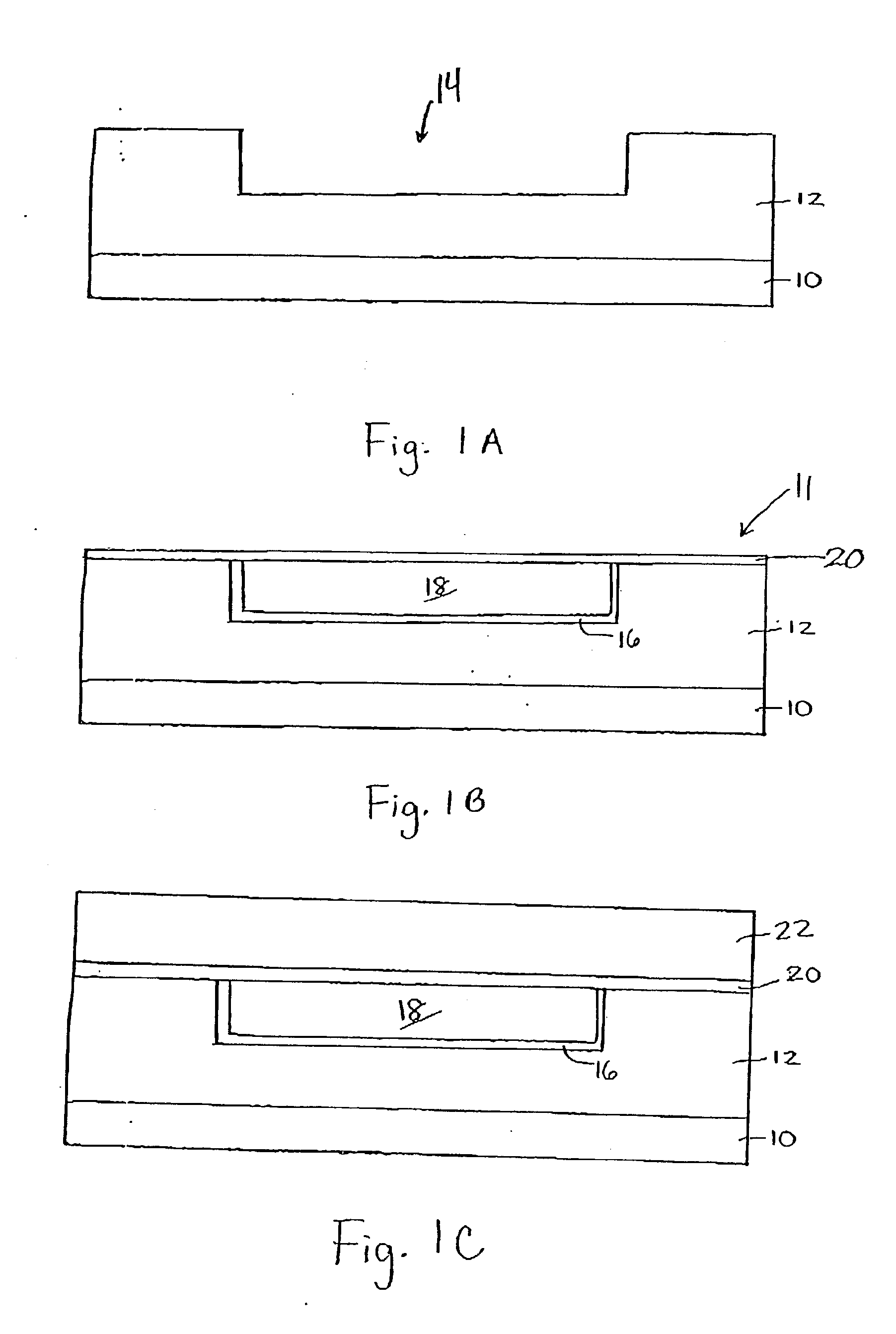
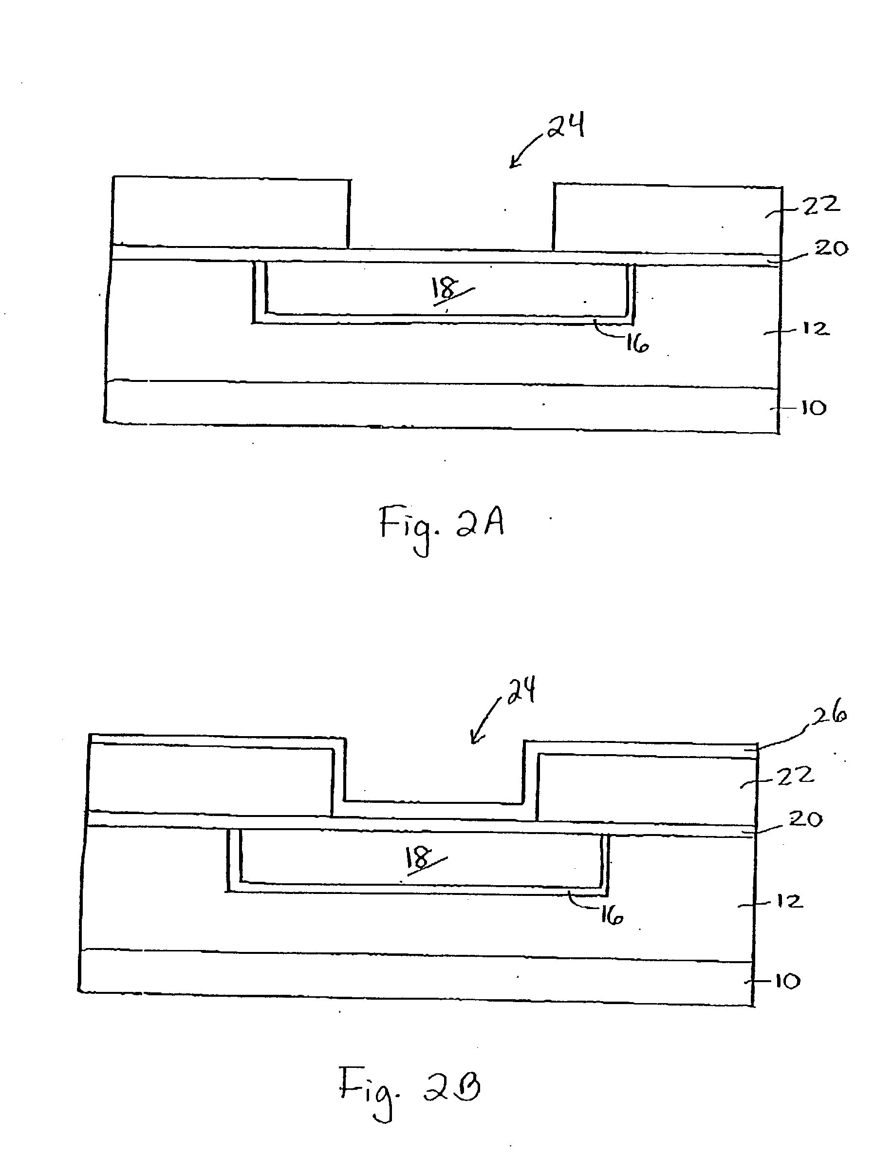
[0036] In describing the preferred embodiment of the present invention, reference will be made herein to FIGS. 1A-7D of the drawings in which like numerals refer to like features of the invention. Features of the invention are not necessarily shown to scale in the drawings.

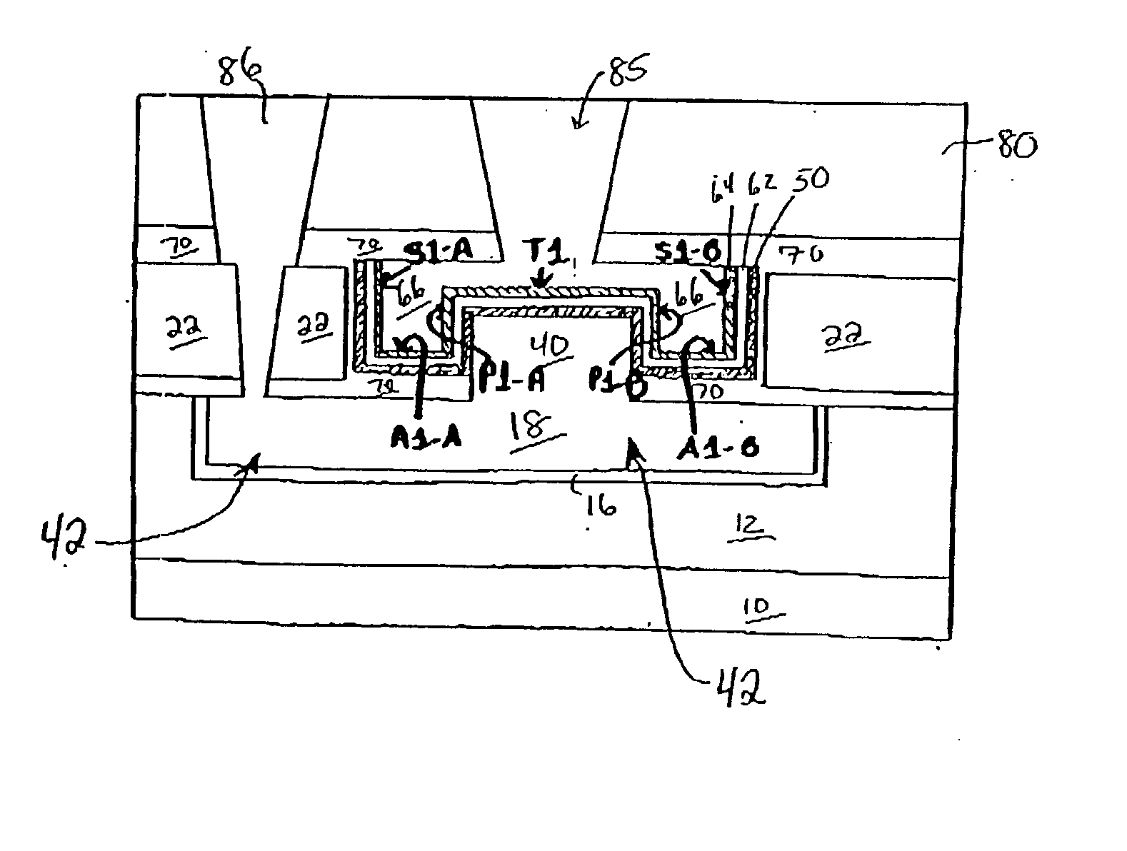
[0037] The instant invention discloses a two lithographic mask method for developing high-k dielectric capacitors using a uniquely modified damascene process that forms conductive pedestals within a trench to increase the surface area of the resultant capacitor. The two masks employed to build the capacitor are required for patterning the trench and the pedestals within the trench. The resultant structure realizes a high-k dielectric capacitor with top and bottom metal electrodes, both preferably comprising low resistivity copper. The use of metal electrodes yields higher voltage linearity over a large voltage range, and improved quality-factors as compared with MOS capacitors. The use of copper plates results in...


PUM


Abstract

The invention is directed to unique high-surface area BEOL capacitor structures with high-k dielectric layers and methods for fabricating the same. These high-surface area BEOL capacitor structures may be used in analog and mixed signal applications. The capacitor is formed within a trench with pedestals within the trench to provide additional surface area. The top and bottom electrodes are created using damascene integration scheme. The dielectric layer is created as a multilayer dielectric film comprising for instance Al2O3, Al2O3/Ta2O5, Al2O3/Ta2O5/Al2O3 and the like. The dielectric layer may be deposited by methods like atomic layer deposition or chemical vapor deposition. The dielectric layer used in the capacitor may also be produced by anodic oxidation of a metallic precursor to yield a high dielectric constant oxide layer.

Description

[0001] 1. Field of the Invention[0002] The present invention relates to semiconductor devices, and in particular, to a capacitor and method of fabricating such capacitor by a damascene process using a pedestal within a trench to increase the surface area of the resultant capacitor.[0003] 2. Description of Related Art[0004] In semiconductor fabrication processes, layers of insulating, conducting and semiconducting materials are commonly deposited and patterned to form integrated circuits (IC). Contact vias, i.e., openings, are also commonly formed in insulating materials known as interlevel dielectrics (ILDs). These vias may then be filled with conductive material to interconnect electrical devices and wiring at various levels.[0005] Damascene processing similarly involves etching trenches in insulating layers in a desired pattern for a wiring layer. These trenches are then filled with conductive material to fill the damascene regions thereby producing integrated wires within the dam...

Claims


Application Information

Patent Timeline
Patent Type & Authority Applications(United States)
IPC IPC(8): H01L21/02H01L21/316H01L21/768
CPCH01L21/31604H01L21/76807H01L28/90H01L28/40H01L28/86H01L21/76831H01L21/0228H01L21/02183H01L21/02258H01L21/022H01L21/02178
Inventor COOLBAUGH, DOUGLAS D.COTTE, JOHN M.ESHUN, EBENEZER E.STEIN, KENNETH J.VAED, KUNALVOLANT, RICHARD P.
Owner GLOBALFOUNDRIES US INC
Why Eureka
Try Eureka