Method for producing material of electronic device

a technology of electronic devices and materials, applied in the direction of solid-state diffusion coatings, chemical vapor deposition coatings, coatings, etc., can solve the problems of deterioration of semiconductor device characteristics, acceleration of deterioration of device characteristics, and increase of electric power consumption, and achieve high-quality effects

Inactive Publication Date: 2004-07-22
TOKYO ELECTRON LTD
View PDF4 Cites 307 Cited by
  • Summary
  • Abstract
  • Description
  • Claims
  • Application Information

AI Technical Summary

Benefits of technology

0011] Another object of the present invention is to provide a process which is capable of providing an electronic device structure comprising an extremely thin (e.g., having a film thickness of 2.5 nm or less) and high-quality oxide film and/or oxynitride film.
0012] A further o

Problems solved by technology

However, when the conventional thin gate insulator is simply intended to be thinned so as to provide a thickness thereof of 2.5 nm or less, the leakage current passing through the gate insulator (gate leakage current) becomes strong, and it causes some problems such as increase in the electric power consumption and acceleration of the deterioration in the device characteristics.
In addition, when the conventional thin gate insulator is used, boron atoms which have been incorporated into the gate electrode during the formation of a gate electrode, will penetrate through the SiO.sub.2 film to reach the silicon substrate as the material underlying the gate insulator, to thereby cause a problem of deteriorating the semiconductor device characteristic.
Howe

Method used


Image

  • Method for producing material of electronic device
  • Method for producing material of electronic device
  • Method for producing material of electronic device

Examples


embodiment of

[0119] (One Embodiment of Production Process)

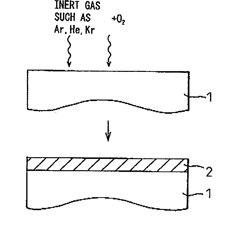
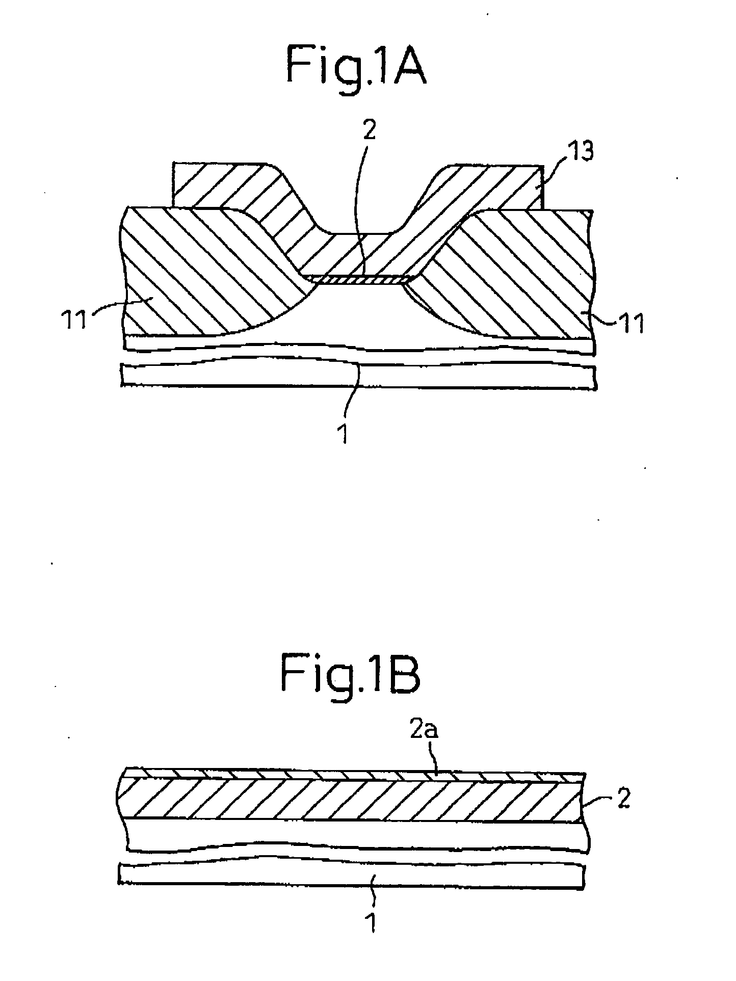
[0120] Next, there is described a process for producing an electronic device material which comprises such an silicon oxide film 2, a nitrided surface portion 2a, and a gate electrode 13 disposed thereon.

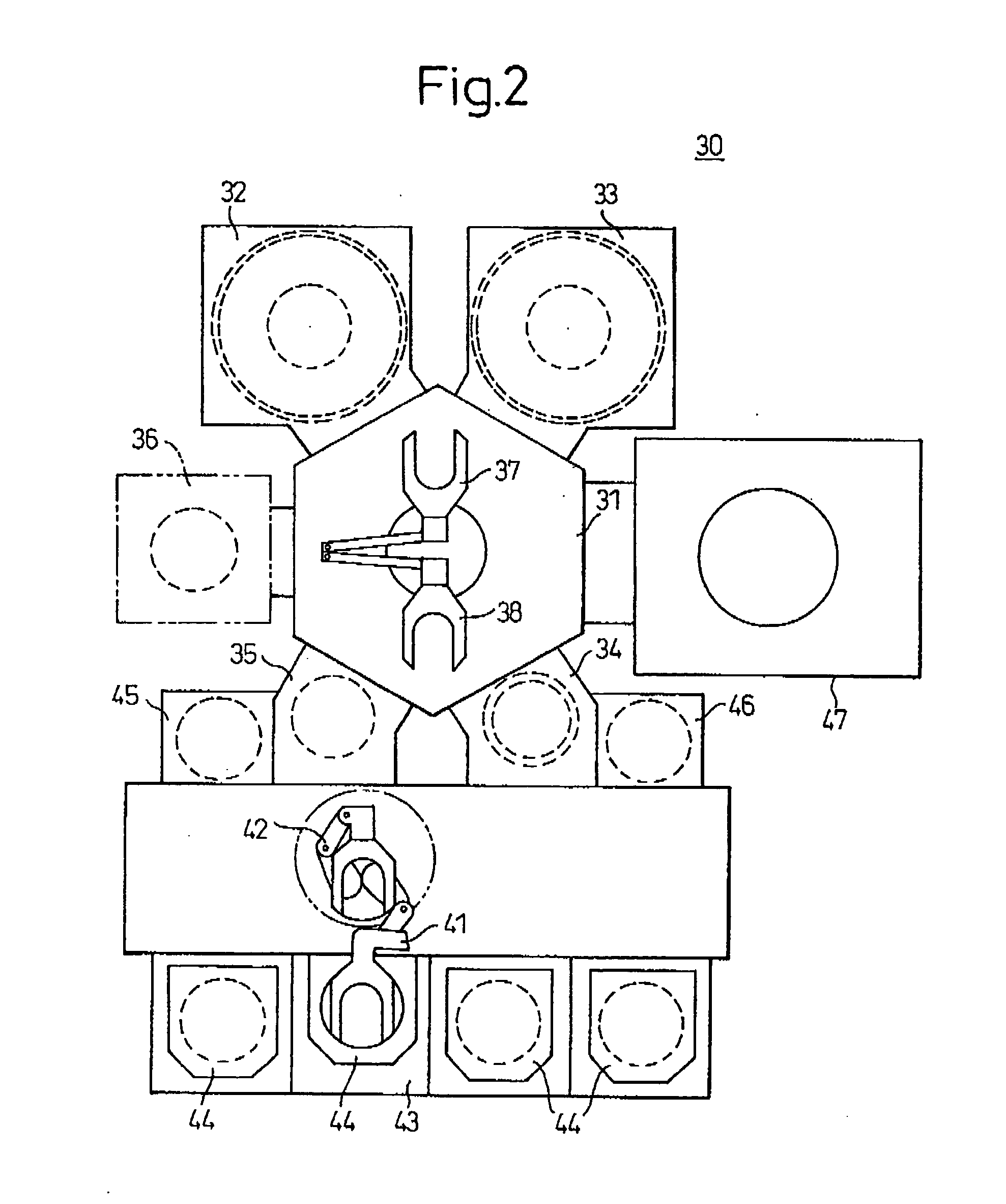
[0121] FIG. 2 is schematic view (schematic plan view) showing an example of the total arrangement of a semiconductor manufacturing equipment 30 for conducting the process for producing electronic device material according to the present invention.

[0122] As shown in FIG. 2, in a substantially central portion of the semiconductor manufacturing equipment 30, there is disposed a transportation chamber 31 for transporting a wafer W (FIG. 3). Around the transportation chamber 31, there are disposed: plasma processing units 32 and 33 for conducting various treatments on the wafer, two load lock units 34 and 35 for conducting the communication / cutoff between the respective processing chambers a heating unit 36 for operating various heating treatm...

examples

[0190] Hereinbelow, the present invention will be described in more detail with reference to Examples.

[0191] By a process for producing electronic device material according to the present invention, an underlying SiO.sub.2 film having a film thickness of 1.8 nm was formed on an N-type silicon substrate which had been subjected to element-isolation formation, by means of an appratus shown in FIG. 2 by using SPA plasma in the process unit 32. The resultant total thickness was 1.8 nm in terms of oxide film thickness (equivalent film thickness). The conditions for the underlying SiO.sub.2 film formation were: O.sub.2 / Ar.sub.2=200 sccm / 2000 sccm, a pressure of 2000 mTorr, a microwave power of 3 W / cm.sup.2, and a temperature of 400.degree. C.

[0192] The conditions for nitriding the underlying SiO.sub.2 film were: N.sub.2 / Ar.sub.2 flow rate=40 sccm / 1000 sccm, a pressure of 7 Pa (50 mTorr), a microwave of 2 W / cm.sup.2, and a temperature of 400.degree. C. The nitridation time was changed so a...


PUM

PropertyMeasurementUnit
Thicknessaaaaaaaaaa
Angleaaaaaaaaaa
Angleaaaaaaaaaa

Abstract

A process for producing electronic device (for example, high-performance MOS-type semiconductor device) structure having a good electric characteristic, wherein an SiO2 film or SiON film is used as an insulating film having an extremely thin (2.5 nm or less, for example) film thickness, and poly-silicon, amorphous-silicon, or SiGe is used as an electrode. In the presence of process gas comprising oxygen and an inert gas, plasma including oxygen and the inert gas (or plasma comprising nitrogen and an inert gas, or plasma comprising nitrogen, an inert gas and hydrogen) is generated by irradiating a wafer W including Si as a main component with microwave via a plane antenna member SPA. An oxide film (or oxynitride film) is formed on the wafer surface by using the thus generated plasma, and as desired, an electrode of poly-silicon, amorphous-silicon, or SiGe is formed, to thereby form an electronic device structure.

Description

[0001] The present invention relates to a process which is suitably usable for the production of materials to be used for electronic devices. The process for producing a material for electronic device according to the present invention may be used, for example, for forming a material to be used for a semiconductor or semiconductor device (for example, those having an MOS-type semiconductor structure).[0002] In general, the production process according to the present invention is widely applicable to the production of materials for electronic device such as semiconductors or semiconductor devices, and liquid crystal devices. For the convenience of explanation, however, the background art relating to semiconductor devices as an example of the electronic devices, will be described here.[0003] Along with the requirement for the fabrication of finer patterns in semiconductor devices in recent years, the demand for a high-quality silicon oxide film (SiO.sub.2 film) has been increased rema...

Claims


Application Information

Patent Timeline
IPC IPC(8): C23C8/02C23C8/34C23C8/36C23C16/44C23C16/455H01L21/314H01L21/316
CPCC23C8/02H01L21/32055C23C8/36C23C16/45565H01L21/0214H01L21/02164H01L21/02238H01L21/02332H01L21/0234H01L21/2807H01L21/28194H01L21/28202H01L21/3144H01L21/31662C23C8/34H01L21/205
Inventor SUGAWARA, TAKUYANAKANISHI, TOSHIOOZAKI, SHIGENORIMATSUYAMA, SEIJIMURAKAWA, SHIGEMITADA, YOSHIHIDE
Owner TOKYO ELECTRON LTD
Why Eureka
Try Eureka