Process and apparatus for producing cystalline thin film buffer layers and structures having biaxial texture

a technology of buffer layers and cystalline, which is applied in the direction of crystal growth process, polycrystalline material growth, superconductor devices, etc., can solve the problems of limiting the effective rate at which biaxial buffer layers are produced, not having the mechanical flexibility and strength needed to scale up the technology for commercial electric power applications, and high cost of single crystal substrates

Inactive Publication Date: 2004-09-02
COMMONWEALTH SCI & IND RES ORG
View PDF15 Cites 51 Cited by
  • Summary
  • Abstract
  • Description
  • Claims
  • Application Information

AI Technical Summary

Benefits of technology

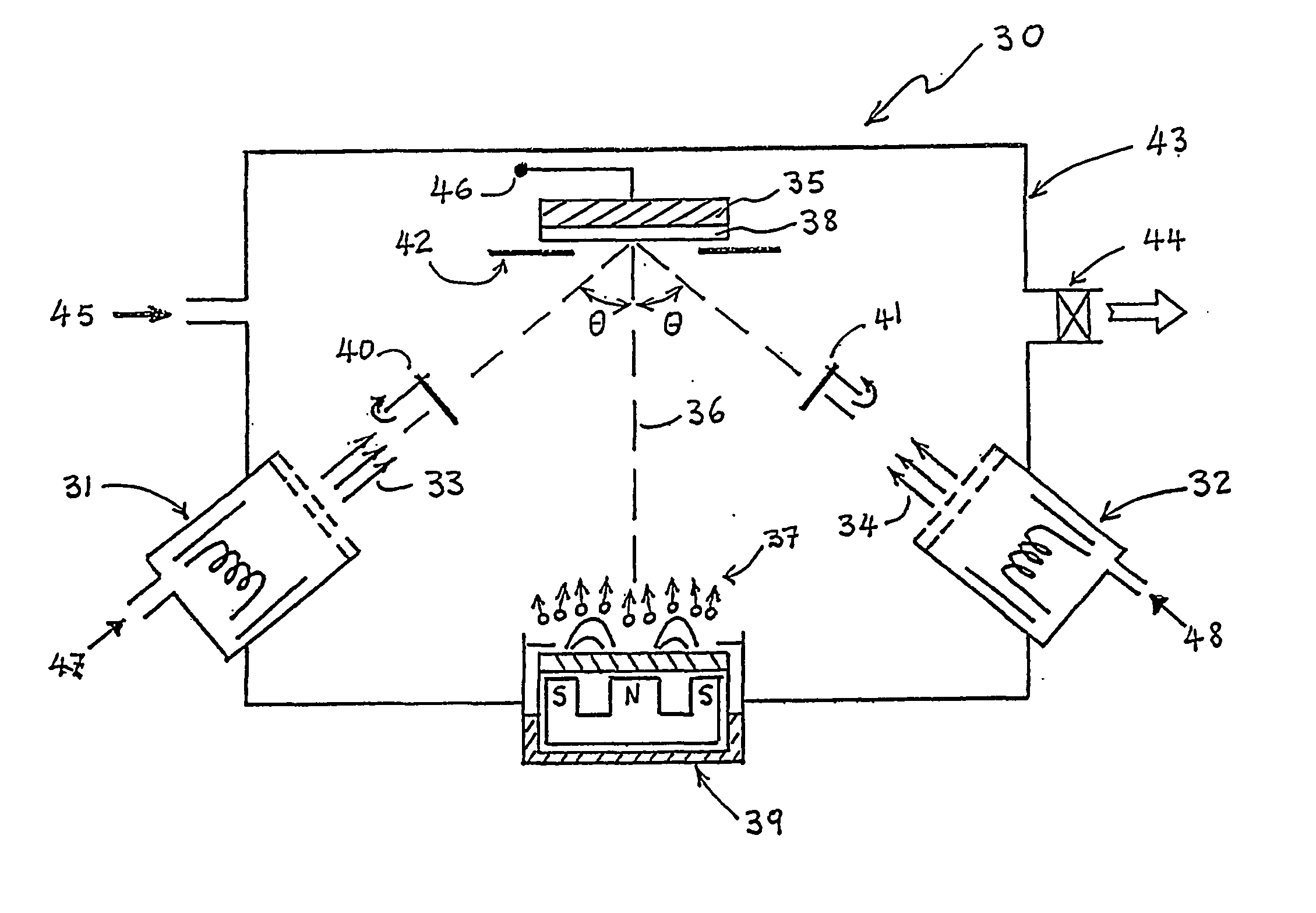
[0021] It has been realised that by providing two or more ion beam sources, a higher deposition rate can be achieved while maintaining an optimum arrival rate ratio. Further, it has been found that the use of two or more ion beams in ion assisted deposition provides a thin film of given thickness with a higher degree of biaxial alignment than such a film formed by known ion beam assisted deposition techniques.
[0029] The method of the first aspect of the present invention may comprise the additional step of negatively electrically biasing the substrate during formation of the film. Negative biasing the substrate can enhance biaxial alignment of the film being formed.
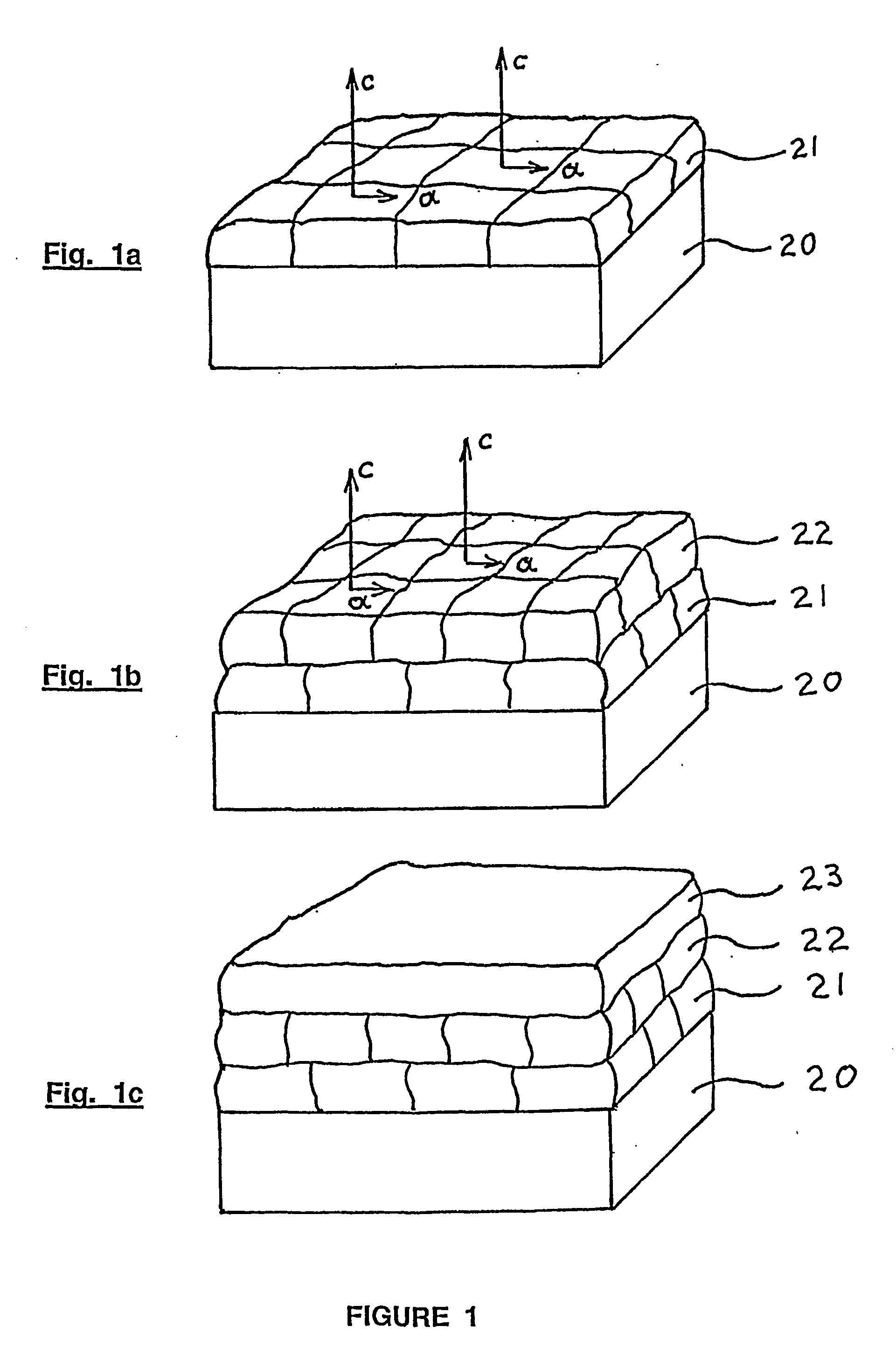
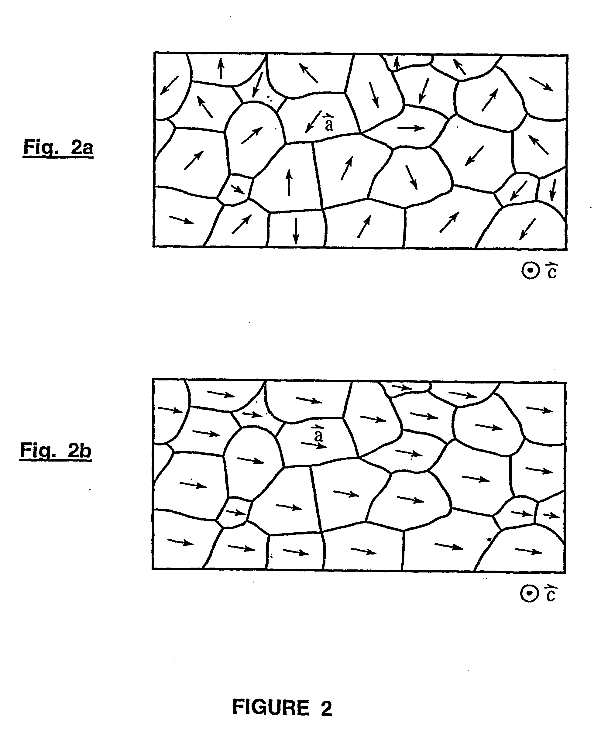
[0037] Embodiments of this invention enable the formation of a film or buffer layer with a thickness from 200 nm to 500 nm or thicker with a high degree of biaxial alignment (.DELTA..phi.<20.degree.), the films having dense microstructure and free of large voids and cracks. Further, the rate of deposition of the present invention can be significantly greater than the rate obtained when using prior art ion beam assisted deposition techniques. The biaxial alignment of a buffer layer deposited in accordance with the present invention, measured by x-ray techniques, can be significantly improved from that of a buffer layer of the same composition deposited under similar conditions but using prior art deposition techniques. Additionally, sequential ion beam bombardment using the present invention can enhance the crystalline quality in the c-axis direction (ie. improves FWHM of omega scans) and can minimise the out-of-plane or c-axis tilt of crystallites, and the biaxial alignment of buffer layers may be further enhanced by applying a negative bias to the substrate.

Problems solved by technology

These single crystal substrates, however, are expensive and can not be produced in large areas or commercial lengths, and do not possess the mechanical flexibility and strength needed to scale up the technology for commercial electric power applications.
This re-sputtering problem and the need to operate within a narrow window of arrival rate ratio place a limit on the effective rate at which biaxial buffer layers are produced.
A further limitation of the IBAD method is that very thick buffer layers (thicker than 500 nm) are required to achieve an acceptable degree of biaxial alignment.
In the prior art, bombardment of a growing film by energetic ions during growth, as occurs in the IBAD process, causes significant re-sputtering of the film, ie. some material is sputtered off and hence lost Consequently, the deposition rate decreases compared to the rate that would be obtained in the absence of the ion beam bombardment.

Method used


Image

  • Process and apparatus for producing cystalline thin film buffer layers and structures having biaxial texture
  • Process and apparatus for producing cystalline thin film buffer layers and structures having biaxial texture
  • Process and apparatus for producing cystalline thin film buffer layers and structures having biaxial texture

Examples


example 2

[0069] Biaxial CeO.sub.2 buffer layers were deposited onto Hastelloy substrates by DIBAD and IBAD (prior art) to compare the degree of biaxial alignment. FIG. 8 shows CeO.sub.2(111) x-ray pole figures and phi scans of the CeO.sub.2 buffer layers, where FIG. 8a relates to the CeO.sub.2 film deposited by IBAD, and FIG. 8b relates to the CeO.sub.2 film deposited by DIBAD. The deposition conditions were: Ar+ ions; angle of incidence .DELTA.=55.degree.; ion beam energy=300 eV; ion to atom arrival rate ratio=0.05. The phi scan peak of the IBAD CeO.sub.2 layer (FIG. 8a) yields .DELTA..phi.=32.degree. while that of the DIBAD CeO.sub.2 layer (FIG. 8b) yields .DELTA..phi.=27.degree.. These results clearly demonstrate that the DIBAD technique yields the sharper biaxial texture. In addition, the phi scans and pole figures of the DIBAD film have a better circular symmetry indicating a lower tilt of the out-of-plane or c-axis orientation compared to the IBAD film.

example 3

[0070] Biaxial YSZ buffer layers were deposited by the DIBAD method onto Hastelloy substrates as a function of ion beam energy. The films were bombarded during growth by Ar+ ions at angle of incidence .theta.=55.degree. and energy in the range from 100 to 400 eV. FIG. 9 shows the YSZ(111) x-ray phi scans and pole figures, where FIG. 9a is for beam energy of 100 eV, FIG. 9b is for beam energy of 200 eV, FIG. 9c is for beam energy of 300 eV, and FIG. 9d is for beam energy 400 eV. The results demonstrate that a sharp texture is obtained at the higher energies.

example 4

[0071] Biaxial YSZ buffer layers were deposited onto Hastelloy substrates by the sequential DIBAD method where each ion beam bombarded the film for periods of 10 to 60 minutes. FIG. 10 shows YSZ(111) x-ray phi scan and pole figures of a typical film 300 nm thick deposited for a total time of two hours where each ion beam bombarded the film for 30 minutes at a time. The other deposition conditions were: Ar+ ions; angle of incidence .theta.=55.degree.; ion beam energy=200 eV; ion to atom arrival rate ratio=0.04.


PUM

PropertyMeasurementUnit
angleaaaaaaaaaa
angleaaaaaaaaaa
energyaaaaaaaaaa

Abstract

The invention provides a method of depositing a buffer layer or film onto a surface of a substrate. The method includes providing the substrate in a controlled atmosphere and exposing the substrate to a vapour comprising a film forming species. While the substrate is exposed to the vapour, two or more ion beams are provided incident upon the surface of the substrate to assist formation of the film. The respective axes of incidence of the two or more ion beams are distinct and are selected and controlled in order to maintain the arrival rate ratio, maximise the deposition rate, and maximise the biaxial alignment of the layer so formed.

Description

[0001] The present invention relates to a method and apparatus for coating a substrate with a biaxially textured thin film buffer layer or layers and articles made thereon, and more specifically to such buffer layers and structures deposited on a substrate to form an article.DESCRIPTION OF THE PRIOR ART[0002] There has been intense effort since the discovery of high temperature superconductors (HTS) to develop processes and apparatus to produce well oriented superconducting filaments supported by or embedded into metallic materials for purposes such as construction of large-scale electrical power devices such as transmission cables and transformers, windings for electric motors, coils for magnets and electrical power storage devices. A parallel effort has concentrated on developing HTS thin films and structures for applications in electronics such as use in magnetic field sensors, and applications in wireless telecommunications including microwave filters and high-Q oscillators.[000...

Claims


Application Information

Patent Timeline
Patent Type & Authority Applications(United States)
IPC IPC(8): C23C14/08C23C14/34C30B29/22C23C14/48C30B23/02H01L39/24
CPCC23C14/083C23C14/3442H01L39/2461C30B29/16C30B23/02C30B23/002H10N60/0632
Inventor SAVVIDES, NICHOLASGNANARAJAN, SABARATNASINGAMKATSAROS, ALEX
Owner COMMONWEALTH SCI & IND RES ORG
Why Eureka
Try Eureka