Analog circuit and display device using the same

a technology of analog circuits and display devices, applied in solid-state devices, amplifiers with semiconductor devices/discharge tubes, instruments, etc., can solve the problems of low mobility of tft formed by using amorphous silicon, long time for making compensation until the original operation, and inability to flow much curren

Active Publication Date: 2004-09-16
SEMICON ENERGY LAB CO LTD
View PDF4 Cites 38 Cited by
  • Summary
  • Abstract
  • Description
  • Claims
  • Application Information

AI Technical Summary

Problems solved by technology

The TFT formed by using amorphous silicon, however, has low mobility.
Therefore, it cannot flow much current.
Therefore, it takes long time for making compensation until the original operation starts.
Additionally, a lot of switches and capacitors are required in the aforementioned source follower circuit, which occupy wider area for the layout and may lower the yield.
However, the charge stored in the capacitor 104 may change due to a noise or a leak current.

Method used


Image

  • Analog circuit and display device using the same
  • Analog circuit and display device using the same
  • Analog circuit and display device using the same

Examples


embodiment

[0226] Embodiment Modes 1 to 6.

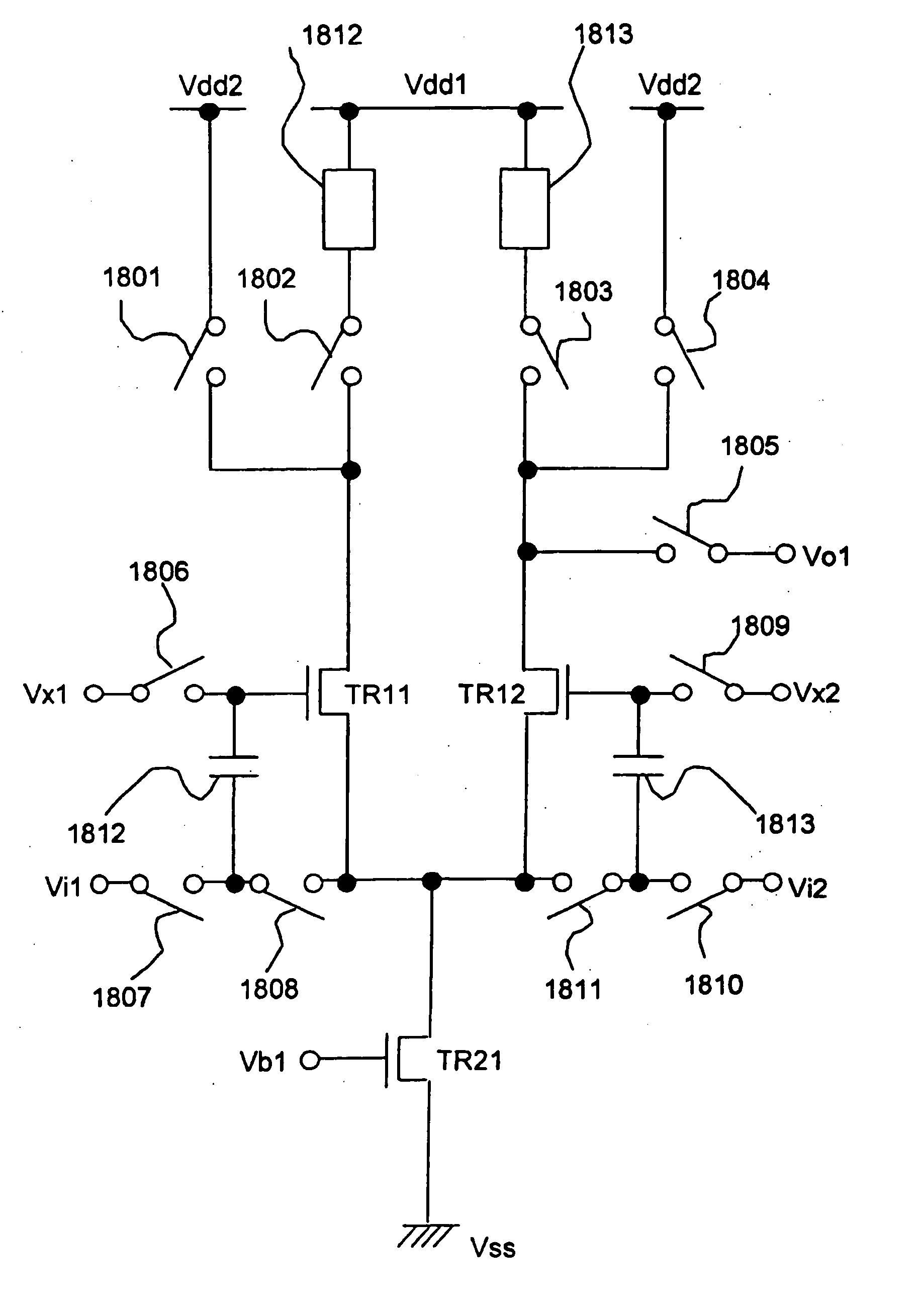
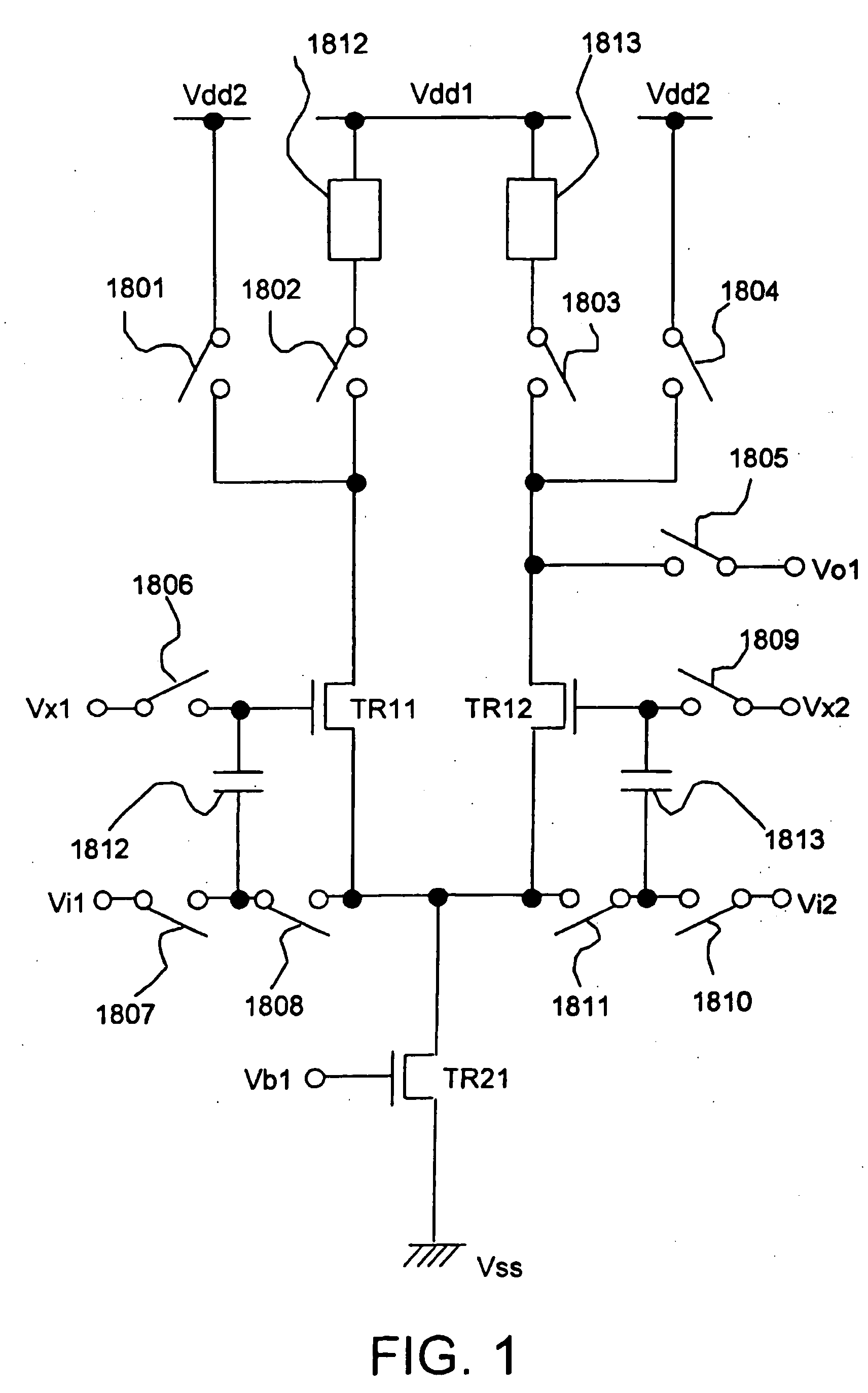
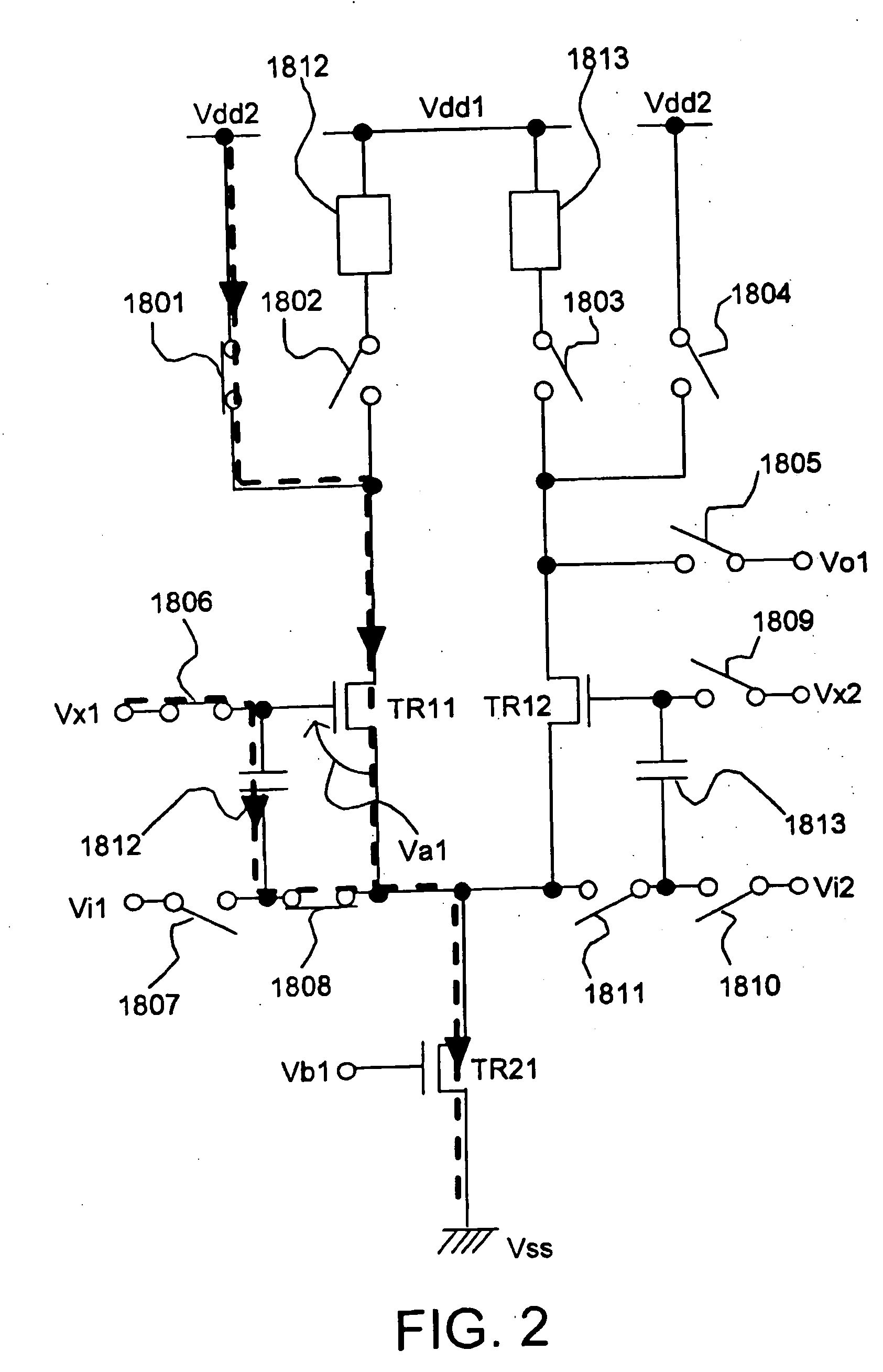
[0227] In the invention, the gate terminal of the transistor is applied voltage in which voltage stored in the capacitor is added to the input voltage, not just the input voltage only. The voltage stored in the capacitor has a potential corresponding to the current characteristics and the size of the transistor. Therefore, when the current characteristics and the size of the transistor vary, the voltage stored in the capacitor changes accordingly. As a result, an effect of variation of the transistor can be decreased.

[0228] An operation to store voltage in a capacitor, that is the compensation operation may be performed at least once. Then, the effect of variation in characteristics of the transistor can be decreased in the subsequent normal operation. Therefore, drive timing is not made complicated and a simple operation can be obtained.

[0229] Moreover, as the numbers of capacitors and switches are small, only a small area is occupied for the layout. ...


PUM


Abstract

The invention provides an analog circuit that decreases an effect of variation of a transistor. By flowing a bias current in a comperisation operation, a voltage between the gate and source of the transistor to be compensated is held in a capacitor. In a normal operation, the voltage stored in the compensation operation is added to a signal voltage. As the capacitor holds the voltage according to the characteristics of the transistor to be compensated, the effect of variation can be decreased by adding the voltage stored in the capacitor to the signal voltage. Further, an analog circuit which decreases the effect of variation can be provided by applying the aforementioned basis to a differential circuit, an operational amplifier and the like.

Description

[0001] 1. Field of the Invention[0002] The present invention relates to an analog Circuit technology. More specifically, the invention relates to a circuit technology to decrease an effect of variation of current characteristics of transistors.[0003] 2. Description of the Related Art[0004] In recent years, a display device having a thin film transistor (TFT) formed on a glass substrate is widely used. For example, a liquid crystal display (LCD) having in each pixel a TFT formed by using amorphous (non-crystalline) silicon is in widespread use in a notebook personal computer or a portable device and the like.[0005] The TFT formed by using amorphous silicon, however, has low mobility. Therefore, it cannot flow much current. In view of the aforementioned, a TFT formed by using polycrystalline silicon is formed on a glass substrate instead. By using the polycrystalline silicon TFT that has high mobility, it is possible to integrate a driver circuit on the glass substrate. A driver circu...

Claims


Application Information

Patent Timeline
Patent Type & Authority Applications(United States)
IPC IPC(8): G11C19/18G11C27/02
CPCG11C19/184G11C27/024H01L27/1255G11C27/028G11C27/026
Inventor KIMURA, HAJIME
Owner SEMICON ENERGY LAB CO LTD
Why Eureka
Try Eureka