Solid-state image sensing apparatus and driving method thereof

a solid-state image and sensing apparatus technology, applied in the direction of television system scanning details, radio control devices, television systems, etc., can solve the problems of large capacitance csp, increased output signal voltage to external noise, and increased chip area, so as to reduce the influence of external noise, reduce the gate size of column selection transistors, and reduce resistance

Inactive Publication Date: 2004-09-23
COLLABO INNOVATIONS INC
View PDF6 Cites 20 Cited by
  • Summary
  • Abstract
  • Description
  • Claims
  • Application Information

AI Technical Summary

Benefits of technology

[0034] Accordingly, it is possible to improve the S / N ratio in the mode in which pixel signals are not summed and the mode in which pixel signals are summed, without enlarging the chip area.
[0036] Accordingly, it is possible to remove fixed pattern noises which are different for each unit cell.
[0041] Accordingly, it is possible to optimize the capacitance of the accumulation capacitor.
[0043] Accordingly, since the column selection transistor is composed of the n-type MOS transistor which has low ON resistance at the time of selecting the column, it is possible to make the gate size of the column selection transistor smaller and to reduce the influence of the external noise from the column selection transistor. Additionally, since the capacitor is composed of the n-type MOS transistor, it is possible to make response characteristic faster. Further, since the capacitor can be formed from one layer of polysilicon not from two layers of polysilicon, it is possible to simplify the manufacturing process.
[0044] By the solid-state image sensing apparatus according to the present invention, it is not necessary to prepare an accumulation capacitor which has a large capacitance in order to sum signal voltage of the unit cell, it is possible to compress images without deteriorating the image quality and enlarging the chip area. Additionally, it is possible to improve the S / N ratio in both of the mode in which pixel signals are summed and the mode in which pixel signals are not summed. Moreover, since it is possible to select the case of summing the signal voltage of the unit cells or the case of not summing signal voltage of the unit cells, it is possible to provide a solid-state image sensing apparatus which corresponds to the case when high pixel value is necessary and the case when minimum pixel value is necessary. Additionally, it is possible to optimize the capacitance of the accumulation capacitor to accumulate the signal voltage of the unit cells.
[0045] Accordingly, it is possible by the present invention to provide a solid-state image sensing apparatus which can compress images without enlarging the chip area and without deteriorating the image quality by a cull. It is also possible to improve the quality of a still image by a camera of a mobile terminal and the camera can correspond to animation and communication. Therefore, its practical value is high.

Problems solved by technology

However, when a conventional solid-state image sensing apparatus does not sum the signal voltage, but accumulates the signal voltage using any of the sampling capacitors 660a, 660b and 660c and outputs the accumulated signal voltage to the horizontal signal line 570, the smaller the sampling capacitance Csp is, the more susceptible is the outputted signal voltage to an external noise caused by ON / OFF of the column selection transistor 650.
Therefore, to restrain the influence of the external noise, it is unavoidable that the sampling capacitance Csp becomes large and there is a problem that the chip area enlarges.
Additionally, when the signals are not summed in the conventional solid-state image sensing apparatus, if a method of using simply a plurality of sampling capacitors is employed, a problem that circuit gain significantly reduces occurs.
However, the gain based on the equation (1) is, on the contrary, Ccp / (Ccp+3 Csp); the circuit gain reduces compared with Ccp / (Ccp+Csp) when one sampling capacitor is used; and transmission efficiency deteriorates.
However, since Ccp, the capacitance of the clamp capacitor at the time, becomes a large value of several pF to several tens of pF, the problem that the chip area enlarges occurs.
However, since the capacitance of the horizontal common signal line is several pF.about.several tens of pF, capacitance of the clamp capacitor Ccp and capacitance of the sampling capacitor Csp becomes extremely large and it is not realistic that the above-mentioned conditions hold.
However, to read out plural times, a problem that the readout time is three times as long as usual occurs.

Method used


Image

  • Solid-state image sensing apparatus and driving method thereof
  • Solid-state image sensing apparatus and driving method thereof
  • Solid-state image sensing apparatus and driving method thereof

Examples


Embodiment Construction

)

[0055] The amplifying-type solid-state image sensing apparatus according to the embodiment of the present invention will be explained below with reference to the figures.

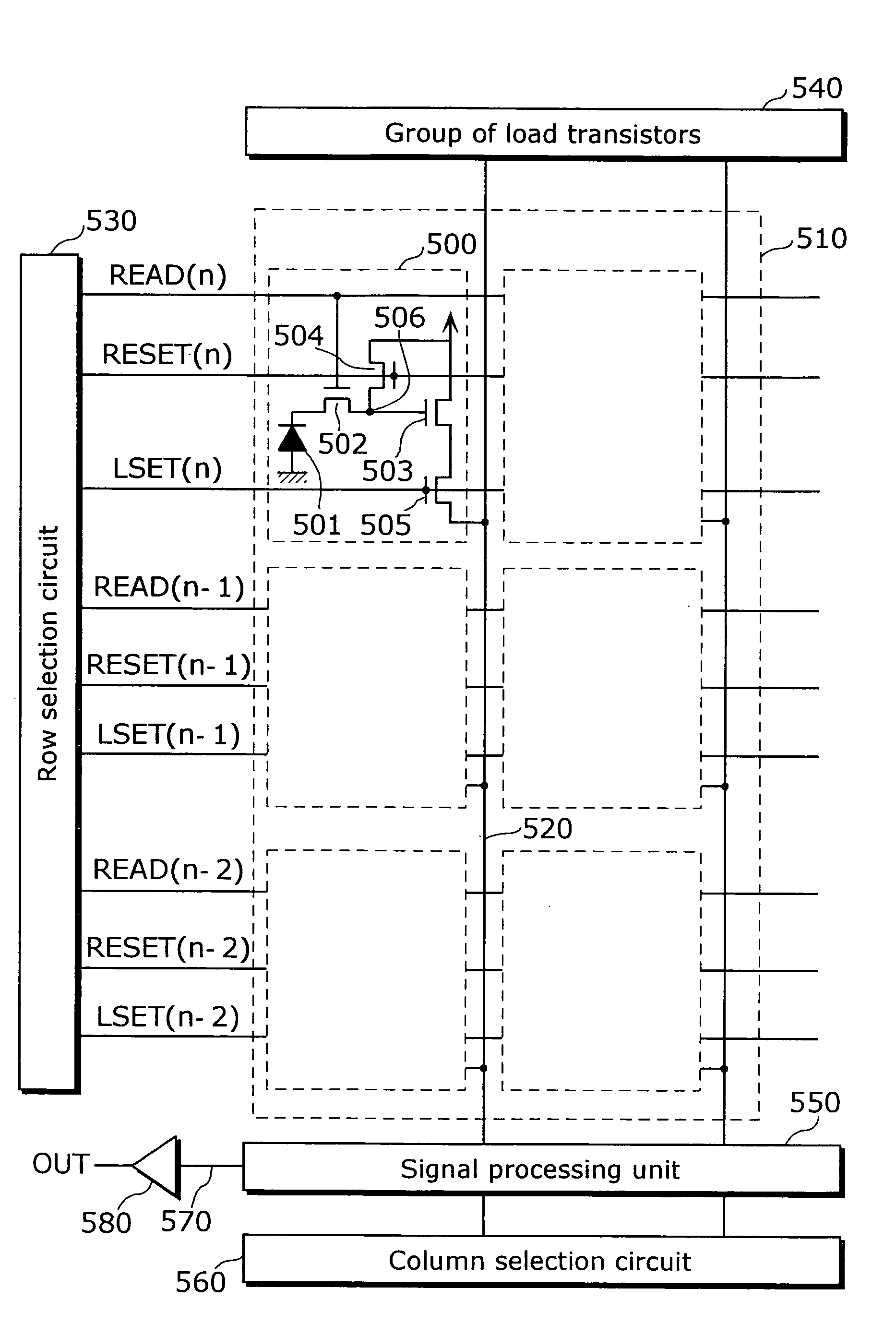
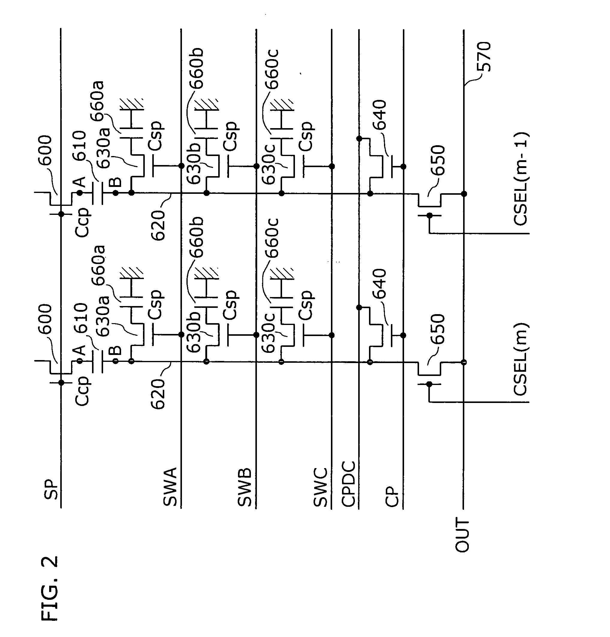
[0056] FIG. 4 is a diagram showing the circuit structure of the amplifying-type solid-state image sensing apparatus according to the present embodiment. It should be noted that in FIG. 4, the same reference numbers are assigned to the same elements in FIG. 1 and their detailed explanations are omitted here.

[0057] The amplifying-type solid-state image sensing apparatus according to the present embodiment aims to realize an amplifying-type solid-state image sensing apparatus which enables to improve the S / N ratio, without enlarging the chip area, in both of a mode in which pixel signals are summed and a mode in which pixel signals are not summed. The amplifying-type solid-state image sensing apparatus according to the present embodiment has a different signal processing unit from the conventional solid-state image se...


PUM


Abstract

A solid-state image sensing apparatus which can improve the S / N ratio without enlarging the chip area in both of the mode in which pixel signals are summed and the mode in which pixel signals are not summed is provided. The solid-state image sensing apparatus includes an image sensing region 510 in which a plurality of unit cells 500 is laid out two-dimensionally, the first vertical signal line 520, a row selection circuit 530, a column selection circuit 560, a horizontal signal line 570 and a signal processing unit 100, having a sampling capacitors which accumulate signals corresponding to amplified signals of the unit cells, which selects the case of summing the signals or the case of not summing the signals, wherein the capacitance of the sampling capacitor which accumulates a signal corresponding to an amplified signal of a unit cell for each row when the sum is performed is smaller than the capacitance required for reading out the signal from said capacitor.

Description

[0001] 1. Field of the Invention[0002] This invention relates to a solid-state image sensing apparatus and particularly to a solid-state image sensing apparatus which can sum pixel signals.[0003] 2. Description of the Related Art[0004] In recent years, in a field of a mobile terminal such as a cellular phone, one with a function to photograph has been widespread. As for the function to photograph which a mobile terminal has, high pixel density (mega pixels) for higher picture quality of a still picture is required and a mobile terminal with the function to photograph is expected to replace a low-cost Digital Still Camera (DSC). On the other hand, the function to photograph which a mobile terminal has is required to be compliant with a picture less than QVGA (about 80,000 pixels), considering animations and communication.[0005] To meet these requirements, in a CCD solid-state image sensing apparatus with high pixel density, so-called mega pixels, for example, removal of pixels by par...

Claims


Application Information

Patent Timeline
Patent Type & Authority Applications(United States)
IPC IPC(8): H01L27/14H01L27/146H01L31/10H04N5/335H04N5/365H04N5/369H04N5/374H04N5/378
CPCH04N5/347H04N5/378H04N5/3575H04N25/46H04N25/616H04N25/75A47G33/00B42D15/00
Inventor MASUYAMA, MASAYUKIMURAKAMI, MASASHI
Owner COLLABO INNOVATIONS INC
Why Eureka
Try Eureka