Semiconductor device and method for manufacturing the same

a technology of semiconductors and semiconductors, applied in the field of semiconductor devices, can solve the problems of inconvenient mass production of substrates, inconvenient use of substrates, and inability to meet the needs of mass production,

Inactive Publication Date: 2004-12-02
SEMICON ENERGY LAB CO LTD
View PDF83 Cites 129 Cited by
  • Summary
  • Abstract
  • Description
  • Claims
  • Application Information

AI Technical Summary

Problems solved by technology

As a substrate for forming these TFTs, a glass substrate or a quartz substrate is widely used now, however, these substrates have some drawbacks such as being fragile and heavy.
Further, these substrates are unsuitable for mass-production since it is difficult to use a large-sized glass substrate or a large-sized quartz substrate.
However, the maximum temperature of the process should be lowered since the heat resistance of a plastic film is low.
As a result, it has been impossible to form a TFT having as good characteristics as that formed over a glass substrate.
Thus, a high-perform

Method used


Image

  • Semiconductor device and method for manufacturing the same
  • Semiconductor device and method for manufacturing the same
  • Semiconductor device and method for manufacturing the same

Examples


embodiment 1

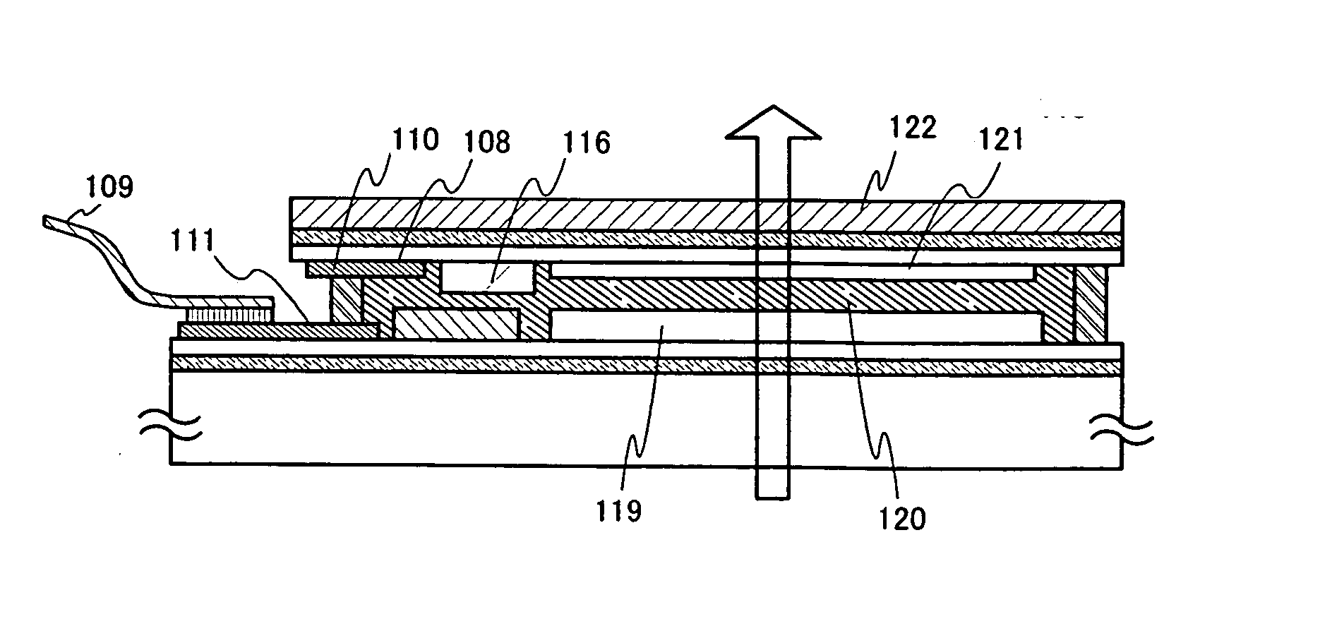
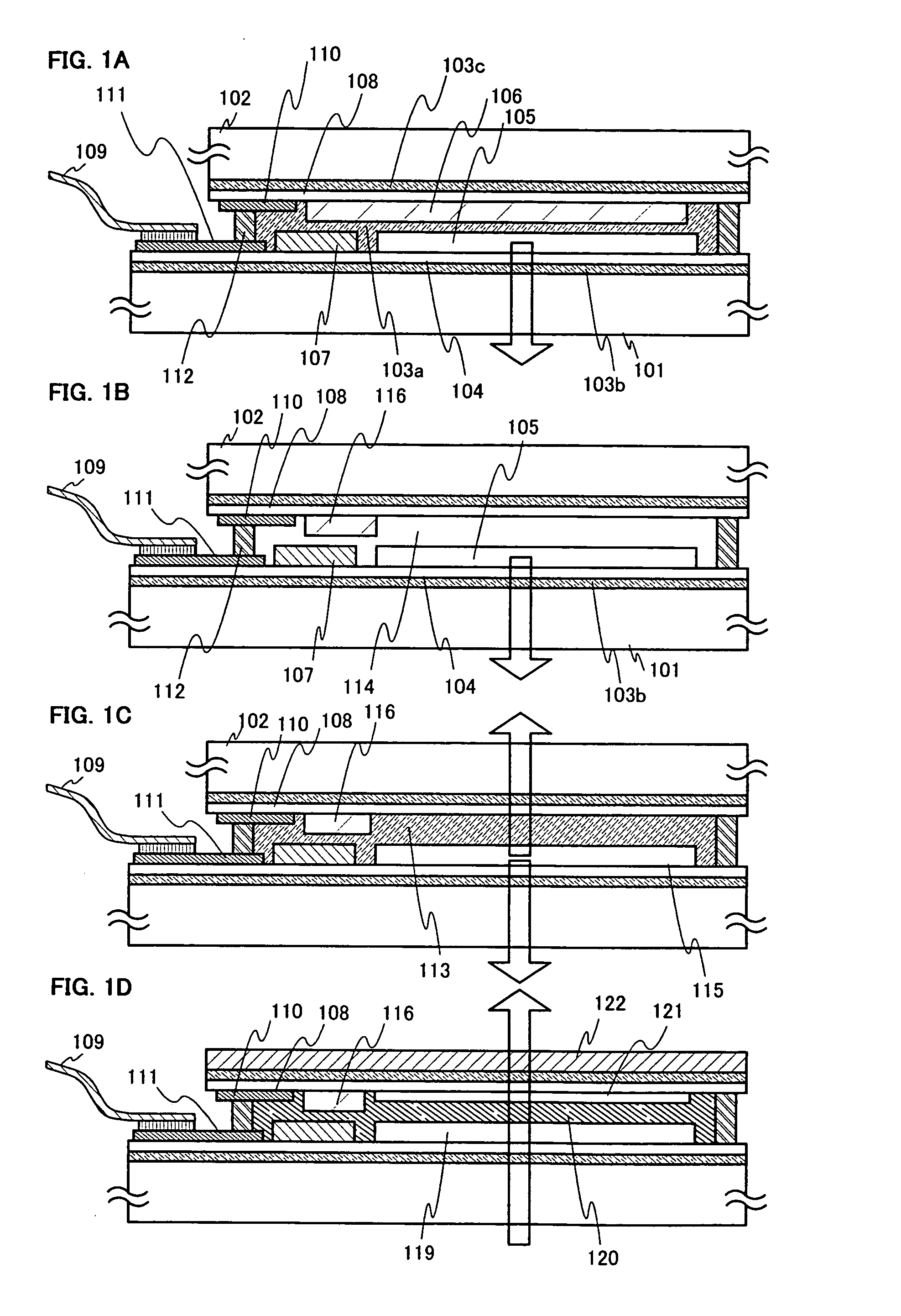
[0109] This embodiment shows an example of manufacturing an assembly of separated layers by the plurality of separated layers obtained by a separation technique and a transfer technique.

[0110] Here, a separation method using a metal film and a silicon oxide film is adopted.

[0111] An element is formed over a glass substrate (a first substrate 200). In this embodiment, AN100 is used as the glass substrate. A metal film 201a is formed, here, a tungsten film is formed as the metal film 201a to have a thickness of from 10 nm to 200 nm, preferably, from 50 nm to 75 nm by sputtering over the glass substrate. Further, an oxide film 202, a silicon oxide film in this instance, is laminated to have a thickness of from 150 nm to 200 nm without being exposed to the air. The oxide film 202 is preferably twice as thick as the metal film or more. It should be noted that a 2-nm to 5-nm-thick metal oxide film (a tungsten oxide film) in amorphous state is formed between the metal film 201a and the sil...

embodiment 2

[0179] This embodiment shows an example of manufacturing a light emitting device (having a top emission structure) provided with a light emitting element that has a layer containing an organic compound as a light emitting layer, over a glass substrate.

[0180] Compared to a bottom emission structure, the top emission structure requires few material layers through which light generated in the layer containing the organic compound pass, thereby reducing stray light between material layers having different reflective index.

[0181] The pixel portion is made up of a plurality of pixels each of which comprises a switching TFT, a current control TFT and a first electrode (anode) which is electrically connected to a drain of the current control TFT. The current control TFT may either be an n-channel TFT or a p-channel TFT, but when it is to be connected to the anode, it is preferably be a p-channel TFT. The TFTs can be manufactured with reference to Embodiment 1. As in Embodiment 1, before the...

embodiment 3

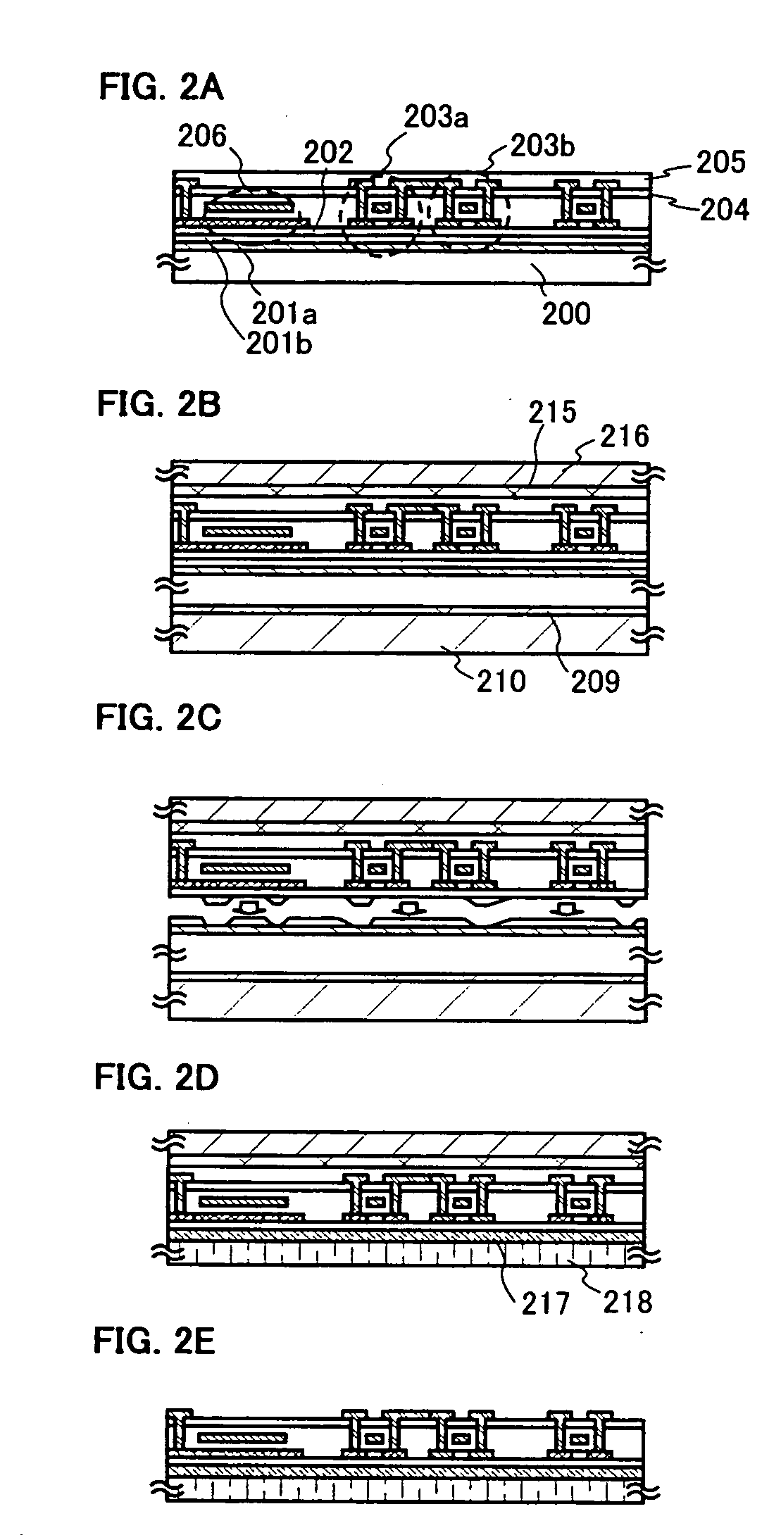
[0191] This embodiment shows an example of a liquid crystal display device hereinafter.

[0192] According to Embodiment 1, a layer to be separated including a pixel TFT is formed over a laminate of a tungsten film, a tungsten oxide film, and a silicon oxide film over a glass substrate. A driver circuit may be formed in the same step. An n-channel TFT is used as the pixel TFT, and a transparent conductive film is used as a pixel electrode. The pixel TFT may be formed by a known method.

[0193] In addition, column spacers containing an inorganic material may be provided at a regular interval to keep the thickness of a liquid crystal layer.

[0194] Subsequently, as in Embodiment 1, the layer to be separated including the pixel TFT is separated from the glass substrate and transferred to a plastic substrate. Thus, an active matrix plastic substrate is manufactured.

[0195] According to Embodiment 1, a layer to be separated including a CPU is formed over a laminate of a tungsten film, a tungsten...


PUM


Abstract

To realize a high-performance liquid crystal display device or light-emitting element using a plastic film. A CPU is formed over a first glass substrate and then, separated from the first substrate. A pixel portion having a light-emitting element is formed over a second glass substrate, and then, separated from the second substrate. The both are bonded to each other. Therefore, high integration can be achieved. Further, in this case, the separated layer including the CPU serves also as a sealing layer of the light-emitting element.

Description

[0001] 1. Field of the Invention[0002] The present invention relates to a semiconductor device having a circuit including thin film transistors (hereinafter, TFT) and a method for manufacturing the same. Specifically, the present invention relates to electronic devices incorporating an electro-optical device typified by a liquid crystal display panel, or a light emitting display device having an organic light emitting element, as a component. In addition, the present invention relates also to a semiconductor device having a circuit including thin film transistors which are formed by transferring and bonding a layer which has been separated by a separation method, to a substrate.[0003] It should be noted that the term "a semiconductor device" in this specification denotes all kinds of devices that can function by utilizing semiconducting properties, and includes all of an electro-optical device, a semiconductor circuit, and electronics.[0004] 2. Description of the Related Art[0005] I...

Claims


Application Information

Patent Timeline
IPC IPC(8): G02F1/1333G02F1/1339G02F1/13G02F1/1345G02F1/1368H01L21/02H01L21/336H01L21/77H01L27/00H01L27/12H01L27/15H01L27/32H01L29/786H01L51/50H01L51/52H01L51/56H05B33/02H05B33/04H05B33/06H05B33/10H05B33/14
CPCH01L27/1214H01L27/1266H01L27/3244H01L27/3276H01L51/5237H01L51/56H01L2221/68368H01L2227/326H01L2251/5323H01L27/1218Y02E10/549Y02P70/50H10K59/12H10K59/131H10K50/8423H10K71/80H10K59/1201H10K50/844H10K2102/3031H10K71/00H10K50/8426H10K77/111H10K50/84H01L29/78672
Inventor TAKAYAMA, TORUMARUYAMA, JUNYAOHNO, YUMIKO
Owner SEMICON ENERGY LAB CO LTD
Why Eureka
Try Eureka