

Method for manufacturing semiconductor device
a manufacturing method and semiconductor technology, applied in the direction of semiconductor devices, electrical devices, transistors, etc., can solve the problems of significant threshold voltage roll-off phenomenon, power consumption increase, and inability to activate boron (b) implanted into the diffusion layer of pmos at such a temperatur
- Summary
- Abstract
- Description
- Claims
- Application Information
AI Technical Summary
Benefits of technology
Problems solved by technology
Method used
Image

Examples
first embodiment
[0037] First Embodiment
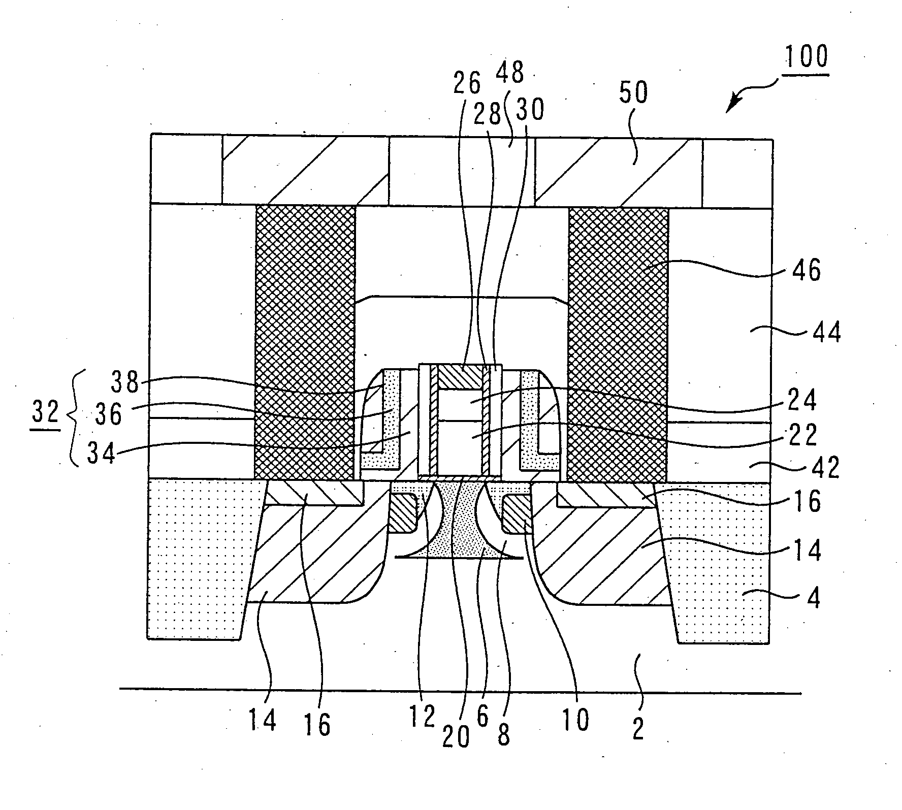
[0038] FIG. 1 is a sectional schematic diagram for illustrating a semiconductor 100 according to the first embodiment of the present invention.
[0039] The semiconductor 100 is a p-channel MOSFET for LOP (low operating power).
[0040] As FIG. 1 shows, a shallow trench isolation (STI) 4 is formed on an Si substrate 2 in the semiconductor 100, an n-well and punch-through stopper 6 are formed in the region partitioned by STI 4, and pocket layers 8 are symmetrically formed on the both side thereof.
[0041] An amorphous region 10 is formed in the vicinity of the surface of the Si substrate 2 on the pocket layers 8. An extension 12 wherein a p-type impurity, such as B ions, is implanted is formed above the amorphous region 10. The extension 12 has a low-concentration impurity diffusion layer having a relatively shallow junction depth of about 10 to 15 nm and relatively low impurity concentration.
[0042] Source-drain regions 14 are formed on the both sides of the extension ...
second embodiment
[0078] Second Embodiment
[0079] FIG. 17 is a sectional schematic diagram for illustrating the semiconductor device 200 according to the second embodiment of the present invention.
[0080] The semiconductor device 200 is a p-channel MOSFET for LOP similar to the semiconductor device 100 described in the first embodiment.
[0081] As FIG. 17 shows, the semiconductor device 200 is similar to the semiconductor device 100. However, in the semiconductor device 200, the gate electrode 54 is not a laminated structure of the SiGe film 22, the Si film 24 and the NiSi film 26; but is a metal gate composed of a TiN film.
[0082] FIG. 18 is a flow diagram for illustrating the method for manufacturing the semiconductor device 200 according to the second embodiment of the present invention. FIGS. 19 and 20 are sectional schematic diagrams for illustrating the states in each manufacturing step of the semiconductor device 200.
[0083] The method for manufacturing the semiconductor device 200 is similar to the...
third embodiment
[0096] Third Embodiment
[0097] FIG. 21 is a sectional schematic diagram for illustrating the semiconductor device 300 according to the third embodiment of the present invention.
[0098] The semiconductor device 300 is a p-channel MOSFET for LOP similar to the semiconductor device 100 described in the first embodiment.
[0099] As FIG. 21 shows, the semiconductor device 300 is similar to the semiconductor device 100. However, the gate insulating film 56 in the semiconductor device 300 is composed of an HfO.sub.2 film, which is a high-dielectric-constant film (High-k film), unlike the semiconductor device 100 wherein the gate insulating film 20 is an SiO.sub.2 film.
[0100] FIG. 22 is a flow diagram for illustrating the method for manufacturing the semiconductor device 300 according to the third embodiment of the present invention.
[0101] The method for manufacturing the semiconductor device 300 is similar to the method for manufacturing the semiconductor device 100 described in the first embo...
PUM
 Abstract
Description
Claims
Application Information