Array comprising organic electronic devices with a black lattice and process for forming the same

a technology of organic electronic devices and black lattices, which is applied in the direction of discharge tubes/lamp details, discharge tubes luminescnet screens, electric discharge lamps, etc., can solve the problems of increasing the thickness of the module, increasing the cost, and not without problems

Inactive Publication Date: 2004-12-23
EI DU PONT DE NEMOURS & CO
View PDF24 Cites 29 Cited by
  • Summary
  • Abstract
  • Description
  • Claims
  • Application Information

AI Technical Summary

Problems solved by technology

However, they are not without problems.
The high reflectivity of the cathode results in poor readability or low contrast of the devices in lighted environments.
However, circular polarizers block about 60% of the emitted light from the OLED and increase module thickness and cost considerably.
The integration of such technology in a full color display and making the final product work in variable environments prove to be difficult.
The interference film also adds manufacturing complexity and reduces yields.
Such complications and perfor

Method used


Image

  • Array comprising organic electronic devices with a black lattice and process for forming the same
  • Array comprising organic electronic devices with a black lattice and process for forming the same
  • Array comprising organic electronic devices with a black lattice and process for forming the same

Examples


example 1

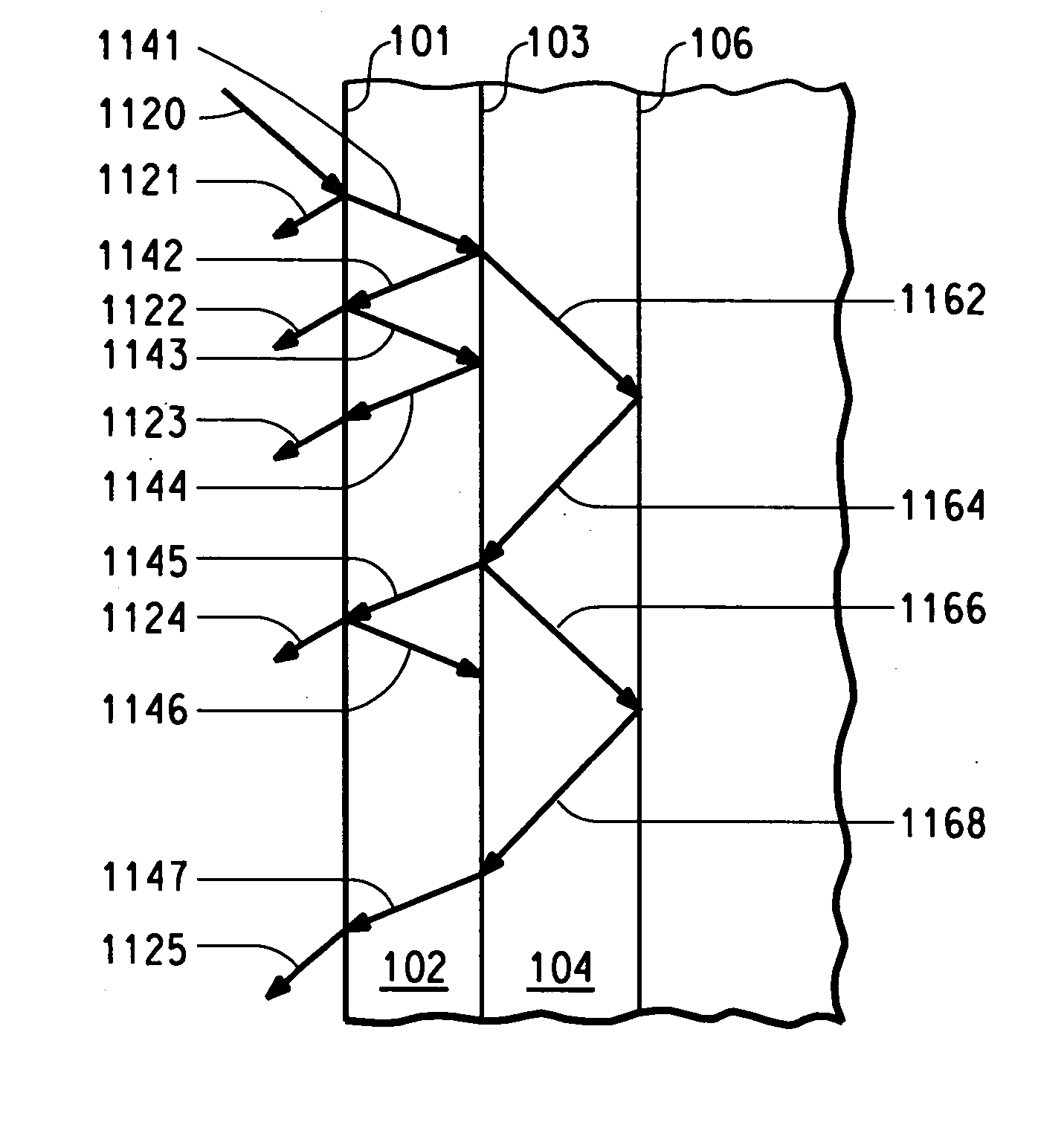
[0113] Example 1 illustrates that a black lattice using a high absorbance material can both increase the contrast and reduce both the radiating and electrical cross talk among electronic devices. In this example, a black lattice is used to reduce L.sub.background and improve CR (Equation 1) by a factor of about two.

[0114] A typical polymer LED is fabricated following well-known procedures. Glass / ITO can be used as substrate and transparent anode. A thin layer of PANI or PEDOT is spin-cast on the substrate, followed by spin-casting an electroluminescent (EL) layer. A thin layer of metal Ba / Al is vacuum deposited on top of EL layer and serves as the cathode. The color of the PLED device depends on the opto-electronic properties of the EL material. The black lattice is fabricated on another glass substrate using photolithography technology. The black lattice could also be fabricated on the device glass substrate. The black lattice is Cr metal which is thick enough to absorb substantial...

example 2

[0115] Example 2 illustrates that a black lattice can be formed on a substrate using a pattern that at least partially surrounds anodes or cathodes. The black lattice fabricated in this way can: 1) enhance the contrast; and 2) eliminate both optical and electronic cross talk between pixels.

[0116] Glass can be used as a substrate. ITO and black photoresist are used as the anode contact and black lattice and are prepared by photolithography in sequence. The ITO is patterned using positive photoresist, and then etching of the ITO. The black lattice is patterned using negative black photoresist. In this example, the black lattice is made as thick as the ITO layer. The lateral dimensions of the black strips are the same as those in Example 1. In fabricating a light emitting device, a thin, transparent PANI or PEDOT layer is spin-cast on the substrate with thickness varied in a range of approximately 30 nm-500 nm. Three different PPV derivatives with EL emission covering the visible range...

example 3

[0118] Example 3 illustrates that OLEDs with black anodes can be fabricated following a similar procedure described in Example 2. This example demonstrates that high display contrast can be obtained with polarizer-less, multicolor organic display with a black anode.

[0119] Glass / Cr / ITO, glass / Ta / ITO, or glass / Si can be used as the substrate and anode, and the anode layers (Cr, Ta, Si, ITO) are prepared by thermal evaporation, MOCVD and PECVD. The reflectivity or transmittance of the anode can be adjusted by the thickness of Cr, Ta, and Si with a light transmission over .about.10%. A thin, transparent PANI layer can be spin-cast with thickness varied in range of 30-500 nm. Three PPV derivatives with EL emission covering the visible ranges is used as the EL layer in three different devices. Their thicknesses are approximately 70 nm. Ba(3 nm) / Al(300 nm) can be used as the cathode layer. A contrast ratio of approximately 100:1 may be obtained for all three different color devices.


PUM


Abstract

An array of electronic devices has an improved contrast ratio by lowering background luminescence from ambient radiation source(s). Background luminescence may be lowered by using a black lattice by itself of in combination with a black layer used between openings in the black lattice. The black lattice, black layer, or both may be achieved by using a high absorbance material, a low reflectivity layer, or a combination of the two. The low reflectivity layer may be designed by optimizing the thickness or materials at the interfaces of the layer to reduce reflectivity. A combination of the black lattice and a black layer within at least one set of the electrodes may provide very low background luminescence while still maintaining a good ratio of ON luminescence versus OFF luminescence.

Description

[0001] This invention relates in general to electronic devices, and more particularly, to an array of organic electronic devices having improved contrast characteristics.DESCRIPTION OF THE RELATED ART[0002] Organic (small molecule or polymer) electroluminescent devices or light-emitting diodes (OLEDs) are promising technologies for flat panel display applications. OLEDs typically include a plurality of electronic device layers including an anode layer, an active layer, and a cathode layer, and may include an optional hole-transport layer, an electron-injection layer, or both. However, they are not without problems. In OLEDs, the cathode is usually made of low work function metals, such as Mg--Ag alloy, Al--Li alloy, Ca / Al, Ba / Al LiF / Al bilayers, and the like, and has mirror-like reflectivity if its thickness is over 20 nanometers. The high reflectivity of the cathode results in poor readability or low contrast of the devices in lighted environments.[0003] An attempt to solve the ref...

Claims


Application Information

Patent Timeline
IPC IPC(8): H01L51/00H01L51/52H05B33/00
CPCH01L51/5284H10K50/865
Inventor YU, GANGSUN, RUNGUANGWANG, JIAN
Owner EI DU PONT DE NEMOURS & CO
Why Eureka
Try Eureka