

Semiconductor device
a technology of semiconductors and devices, applied in the direction of semiconductor devices, laser active region structures, electrical devices, etc., can solve the problems of devices not being able to achieve high-frequency characteristics and high-power characteristics, and achieve the effect of facilitating the formation of via holes
- Summary
- Abstract
- Description
- Claims
- Application Information
AI Technical Summary
Benefits of technology
Problems solved by technology
Method used
Image

Examples
first embodiment
[0053] A first embodiment of the present invention will be described with reference to the associated drawing.
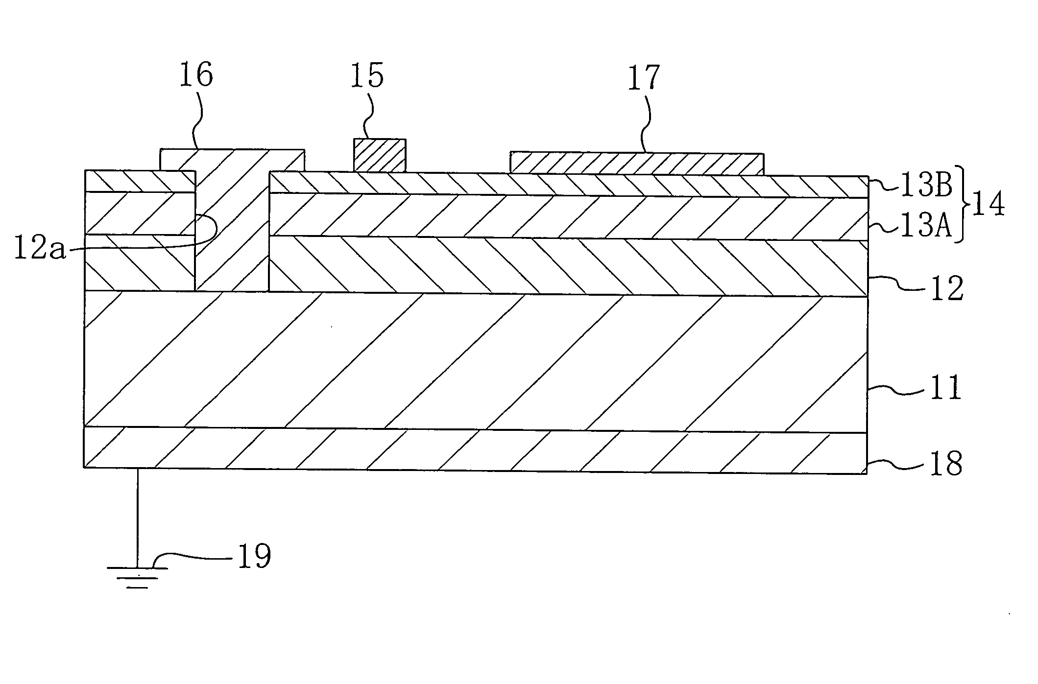
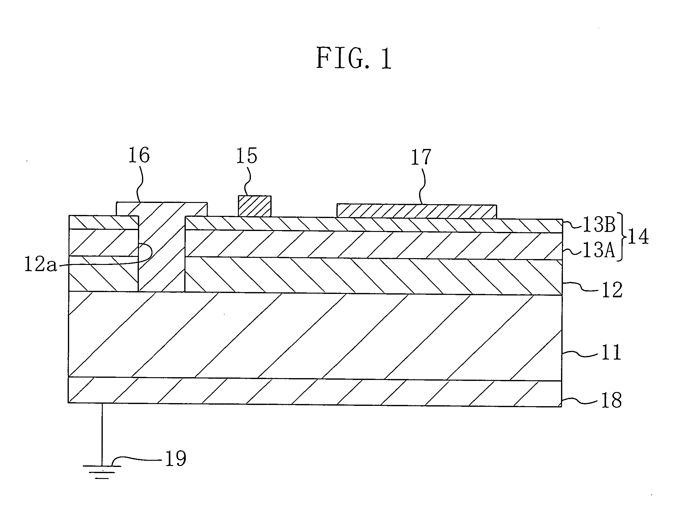
[0054]FIG. 1 illustrates a semiconductor device according to the first embodiment of the present invention, and schematically shows the cross section of a heterojunction field effect transistor (HFET). As shown in FIG. 1, the HFET according to the first embodiment includes: a P+-type conductive substrate 11 made of silicon (Si), for example; a buffer layer 12 as a first semiconductor layer made of a high resistance aluminum gallium nitride (AlxGa1-xN where 0≦x≦1); and an element-forming layer 14 as a second semiconductor layer including a channel layer (active layer) and made of a Group III-V nitride semiconductor. In this embodiment, the conductive substrate 11 is formed so that a dopant concentration of phosphorus (P) or arsenic (As) becomes about 1×1020 cm−3 by ion implantation, for example. Further, the buffer layer 12 is formed so as to reduce lattice mismatch between ...
second embodiment
[0063] Hereinafter, a second embodiment of the present invention will be described with reference to the associated drawing.
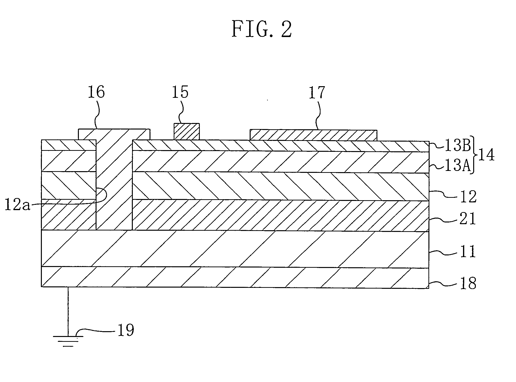
[0064]FIG. 2 illustrates a semiconductor device according to the second embodiment of the present invention, and schematically shows the cross section of an HFET. In FIG. 2, the same constituting members as those shown in FIG. 1 are identified by the same reference characters, and thus the description thereof will be omitted.
[0065] As shown in FIG. 2, the HFET according to the second embodiment is provided, at its portion located between the P+-type conductive substrate 11 and the high resistance buffer layer 12, with at least one depletion-forming layer 21 as a third semiconductor layer which is made of P−-type silicon having a dopant concentration lower than that of the conductive substrate 11, i.e., a resistance higher than that of the conductive substrate 11. In this embodiment, the thicknesses of the high resistance buffer layer 12 and the depletion-form...
first modified example of second embodiment
[0069]FIG. 3 illustrates a semiconductor device according to a first modified example of the second embodiment of the present invention, and schematically shows the cross section of an HFET. In FIG. 3, the same constituting members as those shown in FIG. 2 are identified by the same reference characters, and thus the description thereof will be omitted.
[0070] In the first modified example, the depletion-forming layer 21 is formed so as to have a PN junction of a P-type lower layer 21a and an N-type upper layer 21b. In this case, the thicknesses of the high resistance buffer layer 12 and the depletion-forming layer 21, and the dopant concentrations of the lower layer 21a and the upper layer 21b are preferably set such that a maximum voltage, which can be supported by the buffer layer 12 and the depletion layer extended in the depletion-forming layer 21, becomes higher than a maximum voltage applied to the drain electrode 17.
[0071] Thus, due to the high resistance buffer layer 12 an...
PUM
 Abstract
Description
Claims
Application Information