Semiconductor device and method for manufacturing the same

Inactive Publication Date: 2005-01-06
RENESAS ELECTRONICS CORP
View PDF4 Cites 13 Cited by
  • Summary
  • Abstract
  • Description
  • Claims
  • Application Information

AI Technical Summary

Benefits of technology

[0012] Under such circumstances, it is an object of the present invention to provide a bipolar semiconductor device that is capable of reducing both

Problems solved by technology

However, if the base layer film is thin, the base resistance increases and the breakdown voltage goes low.
Therefore, the base current leakage tends to increase due to the recombination.
It has thus been difficult to reduce the components related to the capacitance.
This method, for the sake of its objective, suffers from a re-distribution of the impurity profile of the intrinsic region, resulting in an impediment to the speedup of the transistor operation.
This also suff

Method used


Image

  • Semiconductor device and method for manufacturing the same
  • Semiconductor device and method for manufacturing the same
  • Semiconductor device and method for manufacturing the same

Examples


Example

FIRST EMBODIMENT

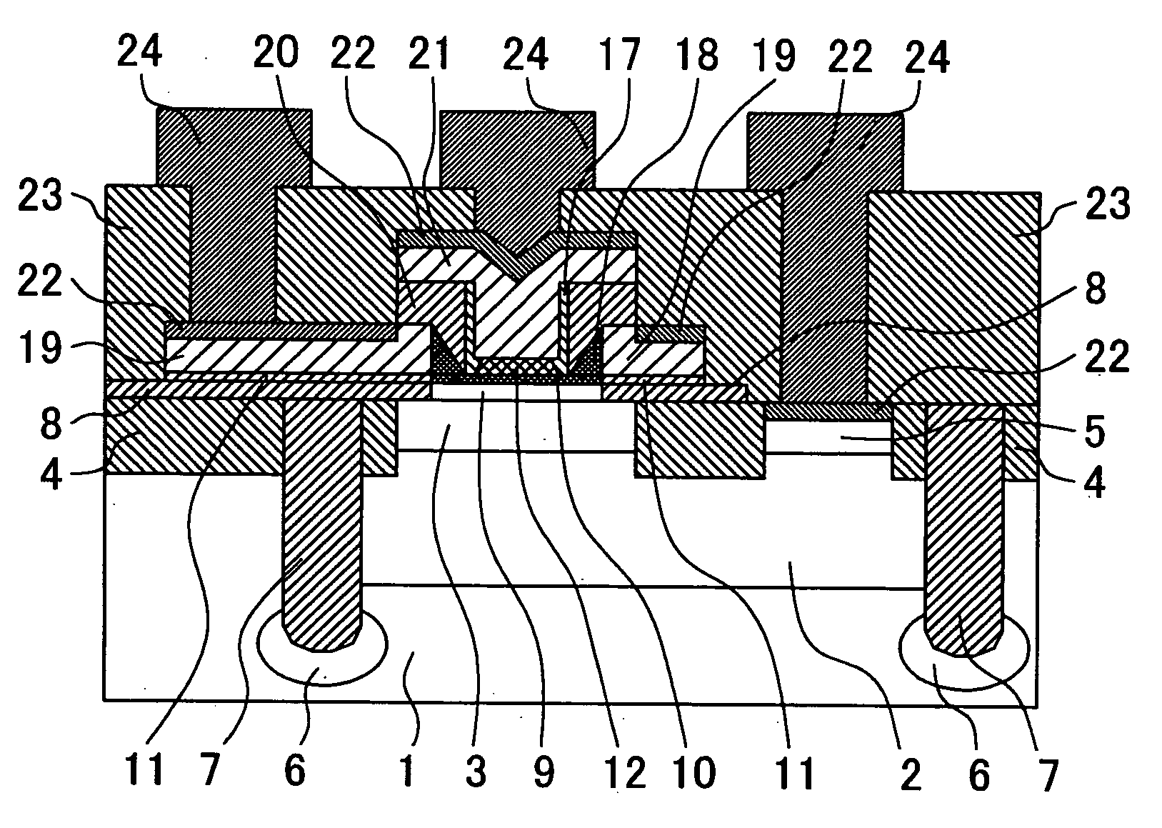
[0051]FIG. 1 shows a cross sectional view of a semiconductor device representing a first embodiment of the present invention. In FIG. 1, the reference numerals and symbols are defined as follows; 1 denotes a p-type silicon substrate, 2 denotes a high concentration collector buried layer, 3 denotes a low concentration collector layer, each of 4, 7, 8, 20, and 23 denotes a silicon oxide film, 5 denotes a collector contact layer, 6 denotes a p-type diffusion layer, 9 denotes a single crystal silicon collector layer, 10 denotes a single crystal silicon base layer, 11 denotes a polycrystalline silicon base, 12 denotes an emitter region, 17 denotes a silicon oxide film sidewall, 18 denotes an extrinsic base, 19 denotes a polycrystalline silicon extrinsic base electrode, 21 denotes a polycrystalline silicon emitter electrode, 22 denotes a silicide layer, 24 to 26 denote an emitter electrode, a base electrode and a collector electrode, respectively.

[0052] Hereinafter, a de...

Example

SECOND EMBODIMENT

[0068]FIG. 12 shows a cross sectional view of a semiconductor device representing a second embodiment of the present invention. In FIG. 12, the same numerals / symbols will be used for the same components as those shown in FIG. 1 and redundant description thereof will be omitted. The bipolar semiconductor device of this second embodiment is provided with a base silicon substrate 31, a silicon oxide film 32, and an n-type silicon layer 33. Those are differences from the configuration of the semiconductor device shown in FIG. 1.

[0069] Hereunder, a description will be given to indicate how to manufacture the semiconductor device of this second embodiment.

[0070] In the method of manufacture of this second embodiment, the substrate to be used first is different from that in the first embodiment. In this second embodiment, a 300 nm silicon oxide film 32 is formed on a base silicon substrate 31, and then a 1000 nm n-type silicon layer is formed thereon. A so-called SOI (S...

Example

THIRD EMBODIMENT

[0072]FIG. 13 shows a cross sectional view of a semiconductor device representing a third embodiment of the present invention. In FIG. 13, the same numerals / symbols will be used for the same components and a redundant description thereof will be omitted. In the bipolar semiconductor device of this third embodiment, the silicon nitride film 34 is provided. This is a difference from the configuration of the semiconductor device shown in FIG. 1. Hereinafter, a description will be given to indicate how to manufacture the semiconductor device of this third embodiment.

[0073] At first, the structure of the semiconductor device shown in FIG. 4 is obtained according to the manufacturing method described in connection with the first embodiment.

[0074] After the structure shown in FIG. 4 is obtained, a 30 nm silicon oxide film 8 and a 15 nm silicon nitride film 34 are deposited. Then, a photo-resist pattern having an opening that is narrower than the low concentration collect...


PUM


Abstract

A bipolar transistor is provided in which both the base resistance and the base-collector capacitance are reduced and which is capable of operating at a high cutoff frequency. The semiconductor device is structured so that the emitter and extrinsic base are separated from each other by an insulator sidewall and the bottom faces of the insulator sidewall, and the emitter are approximately on the same plane. The extrinsic base electrode and the collector region are separated from each other by an insulator.

Description

CLAIM OF PRIORITY [0001] The present application claims priority from Japanese application JP-2000-190752, filed on Jul. 3, 2003, the content of which is hereby incorporated by reference into this application. FIELD OF THE INVENTION [0002] The present invention relates to a semiconductor device , and, more particularly, it relates to a very fast operation bipolar semiconductor device. BACKGROUND OF THE INVENTION [0003] A bipolar transistor, which is formed through silicon selective epitaxial growth and operates as a fast operation bipolar transistor, is disclosed in JP-A 79394 / 1998. (the term “JP-A” as used herein designates an “unexamined published Japanese patent application”). Hereinafter, an example will be described which is referred to as conventional example 1. FIG. 2 shows a cross sectional view of a bipolar transistor constituting the conventional example 1. In FIG. 2, reference numerals and symbols are defined as follows; 101 denotes a silicon substrate, 102 denotes a high...

Claims


Application Information

Patent Timeline
IPC IPC(8): H01L21/331H01L29/732H01L29/737
CPCH01L29/7322H01L29/66287
Inventor OUE, EIJIWASHIO, KATSUYOSHISHIMAMOTO, HIROMIODA, KATSUYAMIURA, MAKOTO
Owner RENESAS ELECTRONICS CORP
Why Eureka
Try Eureka