Adhesive film for use in multilayer printed wiring board and method of producing multilayer printed wiring board

a technology of adhesive film and wiring board, which is applied in the direction of synthetic resin layered products, metal layered products, domestic applications, etc., can solve the problems of high exposure of inorganic filler, large exposure of shape and processing speed, and easy generation of cracks or the like, and achieves the effects of convenient preparation, high resin fluidity, and convenient preparation

Inactive Publication Date: 2005-01-13
AJINOMOTO CO INC
View PDF0 Cites 26 Cited by
  • Summary
  • Abstract
  • Description
  • Claims
  • Application Information

AI Technical Summary

Benefits of technology

[0115] In the layer A and the layer B of the present invention, in addition to the above essential components, if necessary, other thermosetting resins, polymer compounds and additives may be used, to an extent that does not damage the effects of the invention.
[0116] As the thermosetting resin, other than mono-functional epoxy resins as diluent, cyanate ester resins, block isocyanate resins, xylene resins, radical generators, polymerizing resins, and so on can be exemplified.
[0117] Preferable examples of the polymer compound include phenoxy resins, polyimide resins, polyamide imide resins, polyether imide resins, polysulfone resins, polyether sulfone resins, polyphenylene ether resins, polycarbonate resins, polyetheretherketone resins, polyester resins and so on, all having an weight average molecular weight in the range of from 5,000 to 100,000. When the polymer compound is added, there are advantages in that the layers A and B can be easily prepared so that the resin can be suppressed from flowing during the lamination and the preferable fluidity may be obtained.
[0118] In particular, when the adhesive film according to the present invention for use in multilayer printed wiring boards is subjected to vacuum lamination at relatively high temperatures, the fluidity of the resin tends to be too high. However, when the polymer compound is contained in an amount of from 5 to 50% by weight, the layer A and the layer B, can be easily prepared so that the resin can be suppressed from flowing during the lamination and the preferable fluidity may be obtained.
[0119] When the weight average molecular weight is less than 5,000, the fluidity cannot be sufficiently suppressed effect; on the other hand, in the case of exceeding 100,000, when the layer of thermosetting resin composition (layer A and layer B) is formed as resin varnish in which the thermosetting resin composition is compounded with the organic solvent, in some cases, the solubility into the organic solvent deteriorates.
[0120] As the polymer compound, phenoxy resins are particularly preferable. As the phenoxy resins, phenoxy resins such as “Phenototo YP50” (manufactured by Toto Kasei Co., Ltd.), “E-1256” (manufactured by Japan Epoxy Resin Co., Ltd.) and so on, brominated phenoxy resins such as “YPB-40-PXM40” (manufactured by Toto Kasei Co., Ltd.) and so on, and phenoxy resins having a bisphenol S skeleton such as “YL6747H30” (Japan Epoxy Resin Co., Ltd., cyclohexanone varnish of a phenoxy resin made of bisphenol A type epoxy resin “Epicoat 828” and bisphenol S: having nonvolatile component 30% by weight and weight average molecular weight of 47,000) and so on can be exemplified.

Problems solved by technology

When a multilayer printed wiring board has such via structures, there occurs a problem in that since the thermal expansion coefficient of a copper wiring connecting the via holes and that of an insulating layer are very different, cracks or the like are generated in the copper wiring or the insulating layer, when a reliability test such as a thermal cycle test or the like is conducted.
However, when a large amount of inorganic filler is present in the insulating layer, there are problems in via shape and processing speed, because the thermal decomposition temperature upon laser processing is different between the resin and the inorganic filler.
However, when a large amount of inorganic filler is contained in the insulating layer, on a roughened surface, the inorganic filler is exposed a lot.
Accordingly, there is the problem that a conductor layer formed by the plating does not exhibit good adhesion.
However, since the highly classified inorganic filler is expensive, it is desired to use less from this point of view.

Method used


Image

  • Adhesive film for use in multilayer printed wiring board and method of producing multilayer printed wiring board
  • Adhesive film for use in multilayer printed wiring board and method of producing multilayer printed wiring board
  • Adhesive film for use in multilayer printed wiring board and method of producing multilayer printed wiring board

Examples


reference example 1

[0153] Twenty parts of liquid bisphenol A type epoxy resin (“Epikote 828EL” manufactured by Japan Epoxy Resin Co., Ltd. and having an epoxy equivalent of 185), 20 parts of brominated bisphenol A type epoxy resin (“YD-500” manufactured by Tohto Kasei Co., Ltd. and having an epoxy equivalent of 500), 20 parts of cresol novolak type epoxy resin (“EPICLON N-673” manufactured by Dainippon Ink and Chemicals, Inc. and having an epoxy equivalent of 215), and 15 parts of end-epoxidated polybutadiene rubber (“Denarex R-45EPT” manufactured by Nagase Kasei Kogyo K.K.) were dissolved into methyl ethyl ketone under heating with stirring. Thereto, 50 parts of brominated phenoxy resin varnish (“YPB-40-PXM40” manufactured by Tohto Kasei Co., Ltd., containing a nonvolatile component of 40% by weight and having a solvent composition of xylene: methoxypropanol: methyl ethyl ketone=5:2:8), 4 parts of 2,4-diamino-6-(2-methyl-1-imidazolylethyl)-1,3,5-trazine isocyanuric acid adduct (as an epoxy curing age...

reference example 2

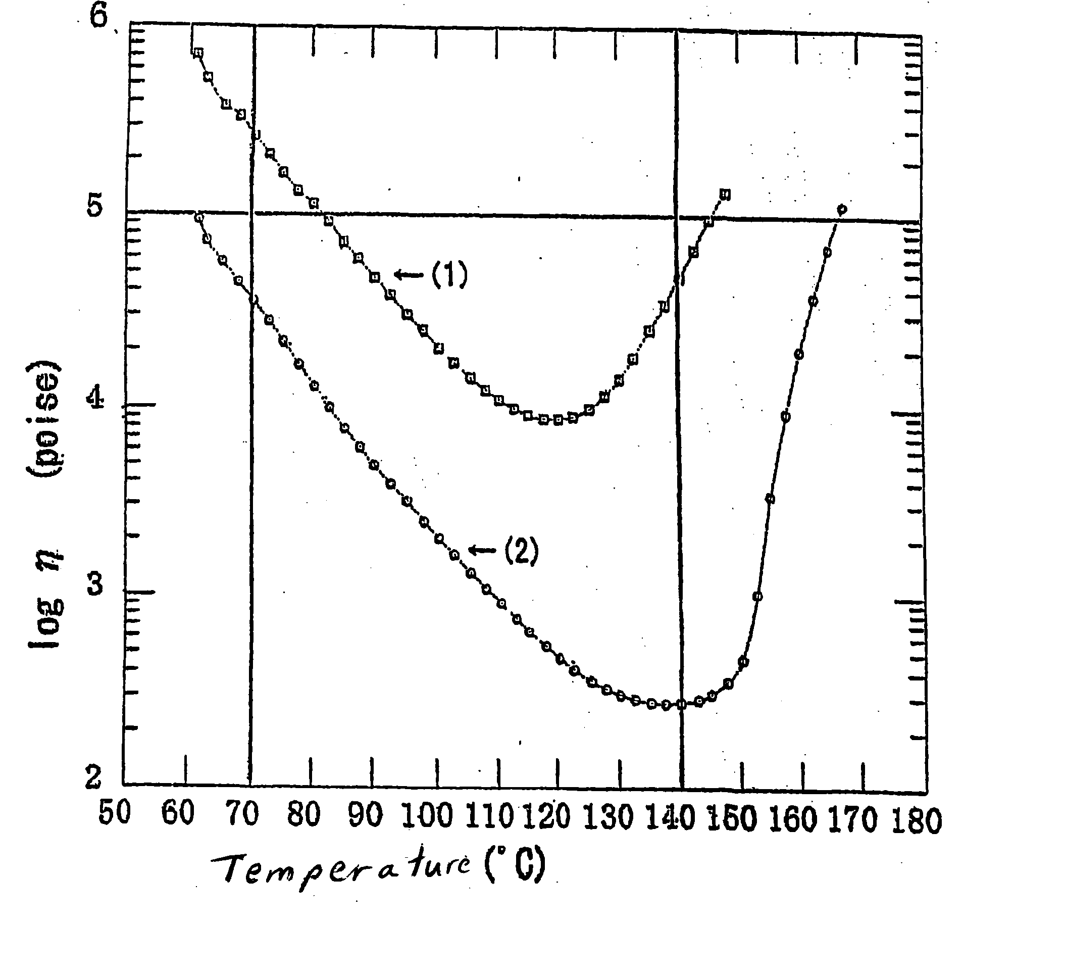
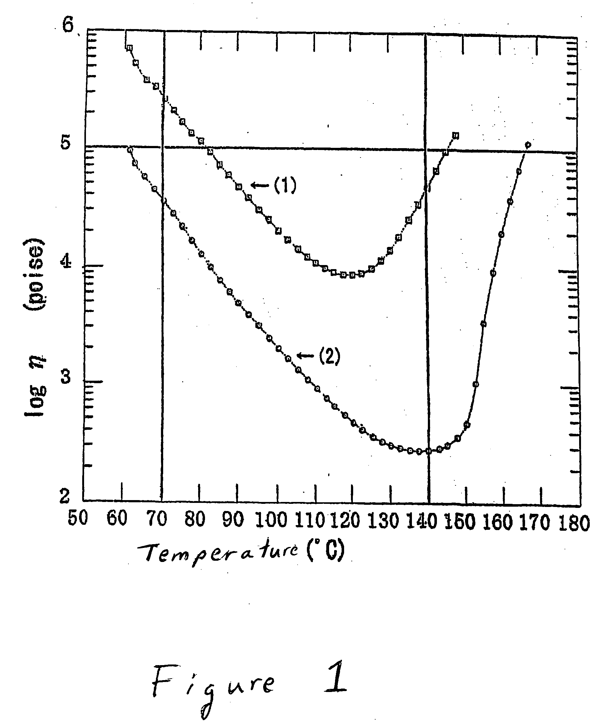
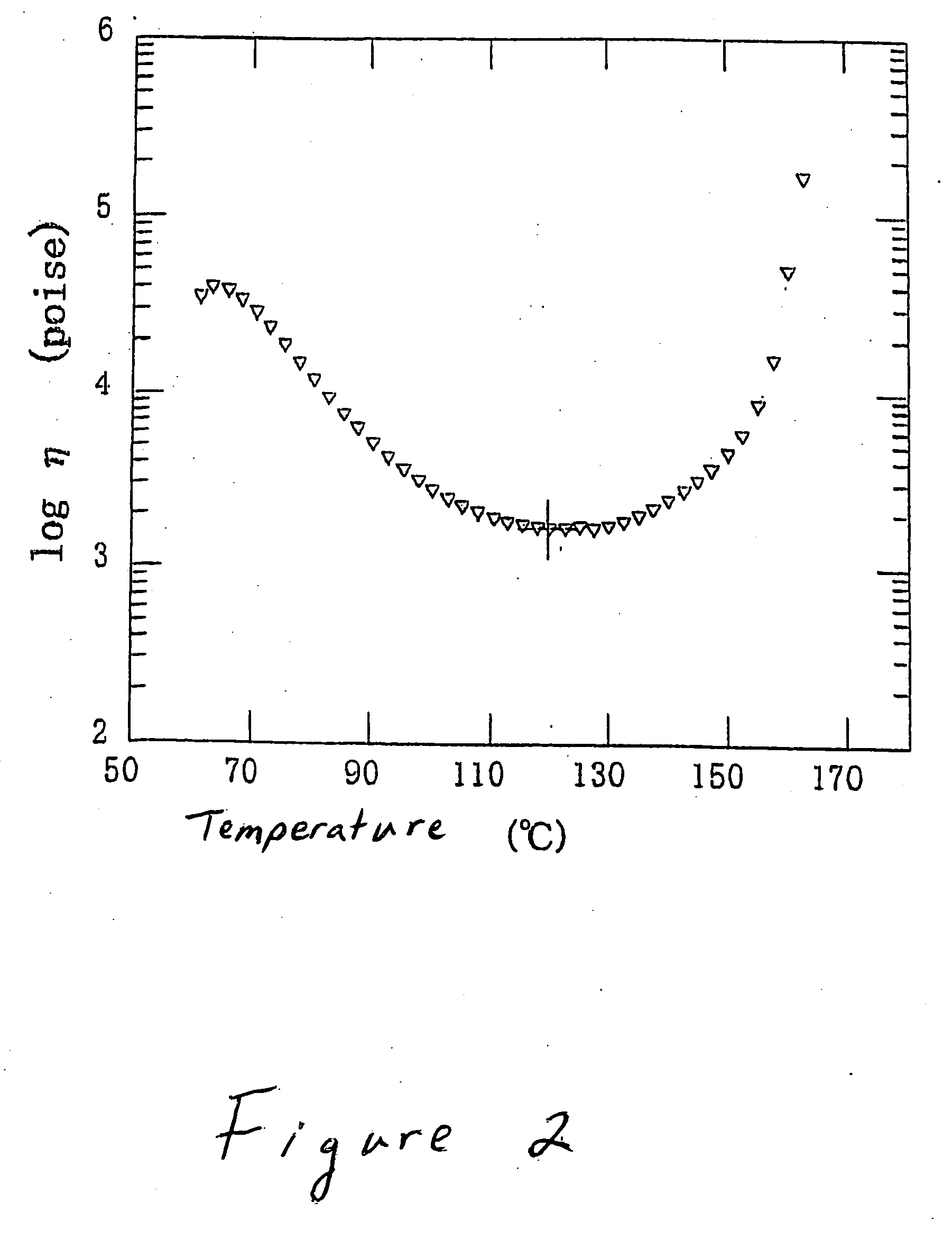
[0157] The dynamic viscoelastic modulus of the thermosetting resin composition made of a layer A and a layer B prepared according to Example 1 described below (two-layered film, having a thickness of: 10 μm+50 μm=60 μm) was measured. The measurements were performed by use of “Dynamic Rheometer Rheosol-G3000” manufactured by UBM Co., Ltd. the same as that used in Reference Example 1. Similarly to Reference Example 1, the measurements were carried out with the temperature rise rate during the measurement set at 5° C. / minute, the measurement starting temperature at 60° C., a measuring temperature interval at 2.5° C., and a vibration at 1 Hz / deg.

[0158] The results are shown in FIG. 2.

example 1

on of an Adhesive Film

[0159] (layer A): Twenty parts of liquid bisphenol A type epoxy resin (“Epikote 828EL” manufactured by Japan Epoxy Resin Co., Ltd. and having an epoxy equivalent of 185), 20 parts of brominated bisphenol A type epoxy resin (“YD-500” manufactured by Tohto Kasei Co., Ltd. and having an epoxy equivalent of 500), 20 parts of cresol novolak type epoxy resin (“EPICLON N-673” manufactured by Dainippon Ink and Chemicals, Inc. and having an epoxy equivalent of 215), and 15 parts of end-epoxidated polybutadiene rubber (“Denarex R-45EPT” manufactured by Nagase Kasei Kogyo K.K.) were dissolved in methyl ethyl ketone under heating with stirring. Thereto, 50 parts of brominated phenoxy resin varnish (“YPB-40-PXM40” manufactured by Tohto Kasei Co., Ltd. containing a nonvolatile component by 40% by weight and having a solvent composition of xylene: methoxypropanol: methyl ethyl ketone=5:2:8), 4 parts of 2,4-diamino-6-(2-methyl-1-imidazolylethyl)-1,3,5-triazine isocyanuric acid...


PUM

PropertyMeasurementUnit
pressureaaaaaaaaaa
pressureaaaaaaaaaa
temperatureaaaaaaaaaa

Abstract

The present invention provides a laminating method, when a multilayer printed wiring board is produced according to a build-up technique, for easily introducing an insulating layer that, under the lamination conditions, allows filling a resin inside a through hole and / or a via hole simultaneously with laminating a circuit board, is low in the thermal expansion coefficient of a formed insulating layer, and, after roughening a surface of the insulating layer, is excellent in the adhesiveness with a conductor layer that is formed according to plating. The present invention also provides a method of forming the insulating layer; and a method of producing the multilayer printed wiring board; and furthermore an adhesive film that is used in these methods. The laminating method is a method of laminating a circuit board characterized in that the adhesive film formed by laminating a resin composition layer made of the following A layer and B layer on a support base film; Layer A is a layer of a thermosetting resin composition that contains an epoxy resin having two or more epoxy groups in one molecule and an epoxy curing agent, has an inorganic filler content of from 0 to less than 40% by weight, has a cured surface obtained by thermally curing which after roughening with an alkaline permanganic acid solution, allows forming a conductor layer according to the plating, and is solid at ambient temperature, and; Layer B is a layer of a thermosetting resin composition that contains an epoxy resin having two or more epoxy groups in one molecule and an epoxy curing agent, has an inorganic filler content of 40% by weight or more, and is solid at ambient temperature; Layer A is laminated adjacent to the support base film; Layer B layer has a fluidity that allows under lamination conditions the filling of a resin into a through hole and / or a via hole simultaneously with the lamination of the circuit board; and The lamination is carried out while keeping the B layer directly in contact with the circuit board.

Description

CROSS REFERENCES TO RELATED APPLICATIONS [0001] This application is a continuation of International Patent Application No. PCT / JP02 / 12442, filed on Nov. 28, 2002, and claims priority to Japanese Patent Application No. 2001-367232, filed on Nov. 30, 2001, both of which are incorporated herein by reference in their entireties.BACKGROUND OF THE INVENTION [0002] 1. Field of the Invention [0003] The present invention relates to methods of producing a multilayer printed wiring board according to a build-up technique in which a circuit-formed conductor layer and an insulating layer are alternately stacked. The present invention also relates to methods of laminating a circuit board with an adhesive film in the production of a multilayer printed wiring board. The present invention further relates to methods of forming an insulating layer by heating and curing a resin composition layer that is introduced after lamination. The present invention also relates to an adhesive film which is useful ...

Claims


Application Information

Patent Timeline
Patent Type & Authority Applications(United States)
IPC IPC(8): B32B7/12B32B15/02H05K3/38H05K3/46
CPCB32B7/12B32B15/02H05K3/387H05K3/4661H05K3/4673H05K2201/0195H05K2201/0209H05K2203/066Y10S428/901Y10T29/49128Y10T29/49155Y10T428/287H05K3/46B32B27/08B32B27/20B32B27/26B32B27/38B32B2457/08
Inventor NAKAMURA, SHIGEOYOKOTA, TADAHIKO
Owner AJINOMOTO CO INC
Why Eureka
Try Eureka