Contact or proximity printing using a magnified mask image

a technology of contact or proximity printing and mask image, which is applied in the field of lithographic methods, can solve the problems of affecting the quality of printed features, the partial abandonment of volume manufacturing techniques, and the increase of pattern transfer process distortion, so as to prevent the adhesion of lens elements

Inactive Publication Date: 2005-01-13
TAKUMI TECH
View PDF5 Cites 54 Cited by
  • Summary
  • Abstract
  • Description
  • Claims
  • Application Information

AI Technical Summary

Benefits of technology

In yet other embodiments of the invention, the method incl

Problems solved by technology

Since the mask image and the wafer image are of the same dimension, this technique was partially abandoned for volume manufacturing because of the tight requirements on the mask image and the difficulty to obtain good contact over the entire wafer area.
As the feature size decreases, distortion in the pattern transfer process becomes more severe.
In the case of OPC, modifications of the design image account for optical limitations as well as mask fabrication limitations and resist limitations.
The destructive interference between adjacent regions of opposite phase creates a very sharp contrast at the boundary between the regions, thus leading to the printing of small features on the wafer.
The main challenge of immersion li

Method used


Image

  • Contact or proximity printing using a magnified mask image
  • Contact or proximity printing using a magnified mask image
  • Contact or proximity printing using a magnified mask image

Examples


Embodiment Construction

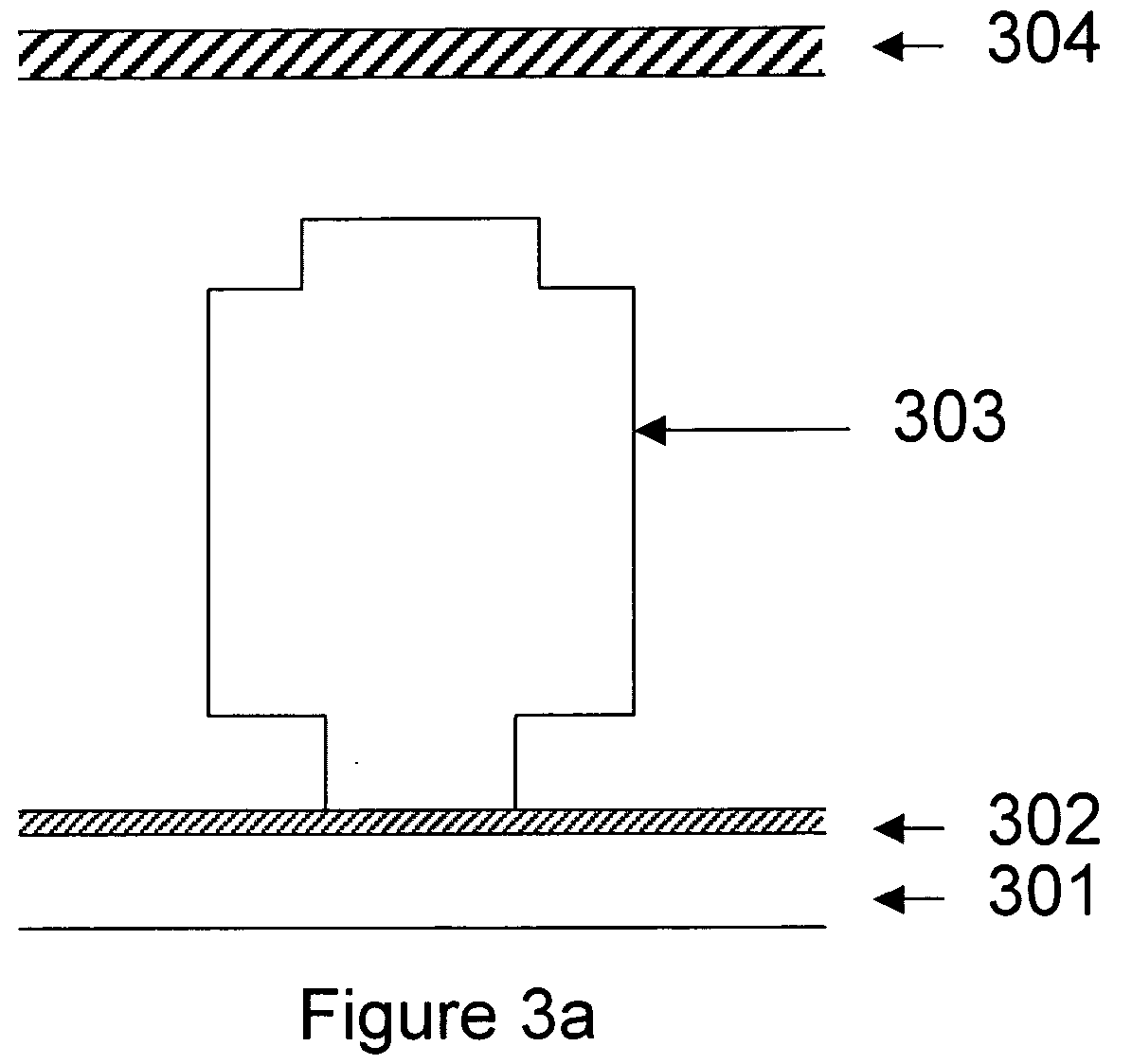
A technique described in FIG. 3a was developed to address the issues encountered with immersion lithography. A wafer 302 is placed on the stage 301. The projection lens 303 projects an image of the mask 304 on top of the wafer 302. The bottom surface of the lens is placed either in close proximity or in contact with the radiation sensitive layer (photoresist) on the wafer 302. Close proximity means that the distance between the bottom of the lens and the wafer is small compared to the wavelength of the exposure, typically smaller than the wavelength divided by 5. The set up described in FIG. 3a will avoid the issue of having a liquid between the lens and the wafer. Moreover, there is no need to insert a solid “immersion” lens between the projection lens and the wafer as the image of the mask 304 is created in the vicinity of the bottom surface (surface facing the wafer) of the last lens element of the projection lens 303. This set up allows the reduction of potential aberrations of ...


PUM


Abstract

Improvements in the fabrication of integrated circuits are driven by the decrease of the size of the features printed on the wafers. Current lithography techniques limits have been extended through the use of phase-shifting masks, off-axis illumination, and proximity effect correction. More recently, liquid immersion lithography has been proposed as a way to extend even further the limits of optical lithography. This invention described a methodology based on contact or proximity printing using a projection lens to define the image of the mask onto the wafer. As the imaging is performed in a solid material, larger refractive indices can be obtained and the resolution of the imaging system can be increased.

Description

FIELD OF THE INVENTION The invention relates to the process of fabricating semiconductor chips. More specifically, the invention relates to a lithographic method. RELATED ART Integrated circuit technology improvements are mostly driven by the decrease of the feature size of the semiconductor chips. As the feature size of the circuit decreases, circuit designers have to deal with the limitations of the lithography process used to manufacture the integrated circuits. The lithography process starts first by coating the surface of the semiconductor wafer with a material called resist. A source of radiation is then shone through the mask in the case of a transparent mask. For a reflective mask the radiation is reflected by the mask. The transparent mask is made of a substrate transparent to the radiation and coated with a patterned opaque layer defining clear and opaque regions to the radiation. Transparent masks are mostly used in optical lithography with typical wavelengths of 436 nm...

Claims


Application Information

Patent Timeline
IPC IPC(8): G03B27/00G03F7/00G03F7/20
CPCB82Y10/00G03F7/70958G03F7/70325
Inventor PIERRAT, CHRISTOPHEWONG, ALFRED KWOK-KIT
Owner TAKUMI TECH
Why Eureka
Try Eureka