
Method for sealing semiconductor component

a technology for semiconductor components and resin compositions, applied in semiconductor devices, semiconductor/solid-state device details, electrical devices, etc., can solve problems such as poor heat resistance of acrylic-modified silicone resin compositions, easy discoloration, and raised problems, and achieve good adhesion and heat resistance.

Active Publication Date: 2005-01-13
SHIN ETSU CHEM IND CO LTD
View PDF2 Cites 53 Cited by
  • Summary
  • Abstract
  • Description
  • Claims
  • Application Information

AI Technical Summary

Benefits of technology

The present invention provides a method for sealing a semiconductor component with an organic resin sealant having heat resistance, transparency, and good adhesion through selective direct imagewise processing. This method allows for sealing at a level of several ten microns and allows for the use of curable organic resin compositions such as silicone and epoxy resin compositions. The resulting sealed components have experienced only a little drop of transmittance during long-term service. The method involves applying a resist material onto the substrate surface, selectively exposing the resist layer to radiation and developing the resist layer with a liquid developer, applying a resin sealant onto the circuit region which is exposed as a result of selective removal of the resist layer and curing the resin sealant, and then removing the residual resist layer using a solvent which can dissolve the resist. The resin sealant is preferably a silicone or epoxy resin composition, which may contain an inorganic phosphor and / or a light scattering agent. The method can be used to seal a semiconductor component with multiple circuit regions and electrodes formed thereon.

Problems solved by technology

The materials of these types are transparent, but raise some problems when used for semiconductor component sealing.
The acrylic-modified silicone resin compositions have poor heat resistance, so that they are likely to discolor on long-term use at elevated temperatures or under ultraviolet exposure.
However, the materials of these types cannot be used when it is desired to seal only selected portions by direct imagewise processing of the material using radiation, typically ultraviolet radiation.

Method used


Image

  • Method for sealing semiconductor component
  • Method for sealing semiconductor component
  • Method for sealing semiconductor component

Examples


example

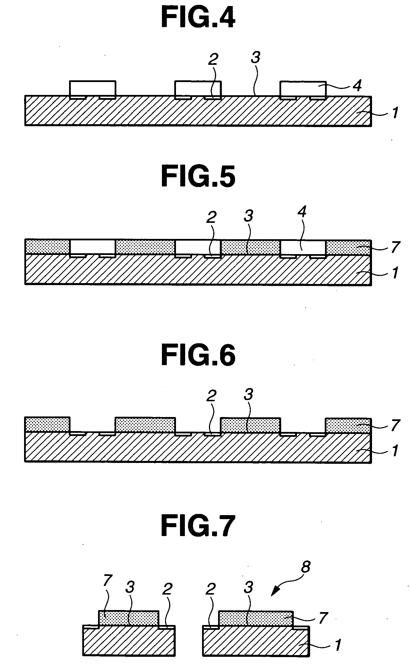
An example of the invention is described with reference to the drawings. FIGS. 1 to 7 illustrate the semiconductor component sealing method of the invention.

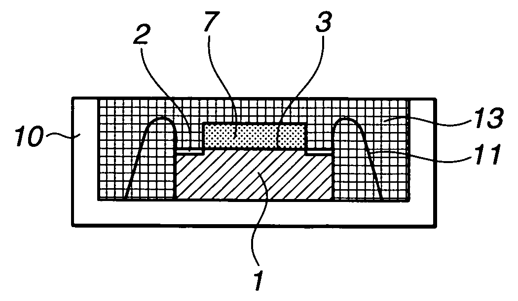
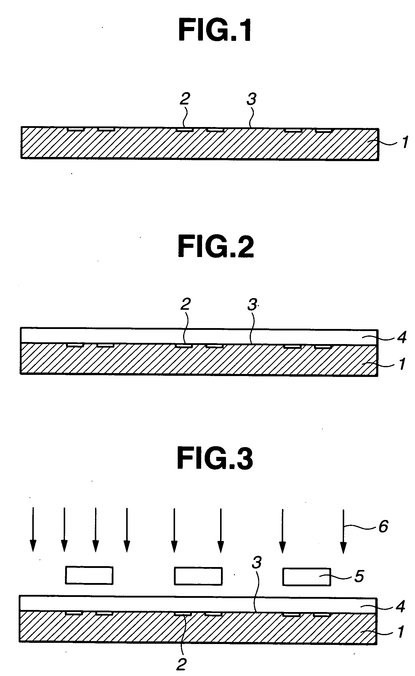
FIG. 1 is a schematic cross-sectional view of one exemplary semiconductor component substrate used in the invention. On the substrate 1, a plurality of circuit regions 3 and electrodes 2 connected thereto had been formed.

A positive resist material SIPR-9271 (Shin-Etsu Chemical Co., Ltd.) was applied onto the surface of the semiconductor substrate 1 by using a spin coater at 2,000 rpm, forming a resist layer 4 of 20 μm thick on the substrate 1 as shown in FIG. 2.

As shown in FIG. 3, a photomask 4 in which light-shielding zones of 3 mm×2 mm were spaced apart at intervals (light-transmissive zones) of 0.5 mm was placed over the substrate 1. Light 6 was illuminated through the photomask 4 whereby only those portions of the resist layer 4 corresponding to the circuit regions 3 were exposed. The light wavelength was 365 nm and th...


PUM


Abstract

In connection with a semiconductor component having a circuit region and electrodes formed on a substrate surface, the circuit region is sealed by (1) applying a resist material onto the substrate surface to form a resist layer, (2) selectively exposing the resist layer to radiation and developing the resist with a liquid developer for thereby removing only the portion of the resist layer which overlies the circuit region, (3) applying a resin sealant onto the circuit region and curing the resin sealant into a cured resin layer that covers the circuit region, and (4) removing the residual resist layer using a solvent.

Description

TECHNICAL FIELD This invention relates to a method for sealing a semiconductor component comprising a substrate and at least one circuit region and electrodes formed on a surface thereof, the circuit region being sealed with a resin. As used herein, the term “semiconductor component” refers to optical semiconductor components as well as ordinary semiconductor components. BACKGROUND ART A traditional method of sealing the surface of a semiconductor component directly with a transparent resin involves using a photosensitive transparent resin, and exposing the resin to radiation through a photomask. The photosensitive resins commonly used in this method are acrylic-modified silicone resin compositions and silicone resin compositions that make use of photo-induced cationic polymerization. The materials of these types are transparent, but raise some problems when used for semiconductor component sealing. The acrylic-modified silicone resin compositions have poor heat resistance, so tha...

Claims


Application Information

Patent Timeline
Patent Type & Authority Applications(United States)
IPC IPC(8): H01L23/28H01L21/44H01L21/56H01L23/12H01L23/31H01L33/50H01L33/56H01L33/62
CPCH01L21/56H01L23/3157H01L33/52H01L2924/12044H01L2924/3025H01L2224/45144H01L2224/48091H01L2924/00014H01L2924/00H01L2224/73265H01L2924/181H01L2924/00012
Inventor SHIOBARA, TOSHIOKASHIWAGI, TSUTOMU
Owner SHIN ETSU CHEM IND CO LTD
Learn More