
Al2O3 atomic layer deposition to enhance the deposition of hydrophobic or hydrophilic coatings on micro-electromechcanical devices

a technology of hydrophilic coatings and atomic layers, applied in the direction of coatings, optical elements, instruments, etc., can solve the problems of deformation significant wear of silicon during the operation of the atomic layer,

Active Publication Date: 2005-01-20
UNIV OF COLORADO THE REGENTS OF
View PDF29 Cites 220 Cited by
  • Summary
  • Abstract
  • Description
  • Claims
  • Application Information

AI Technical Summary

Problems solved by technology

Two significant problems facing MEMS are frictional wear and stiction.
Frictional wear is a common mode of failure and degraded performance for many MEMS.
Silicon may wear significantly during operation of the MEMS device.
Gears and other engaging MEMS components may experience this problem to an even greater extent.
Stiction is another problem facing MEMS.
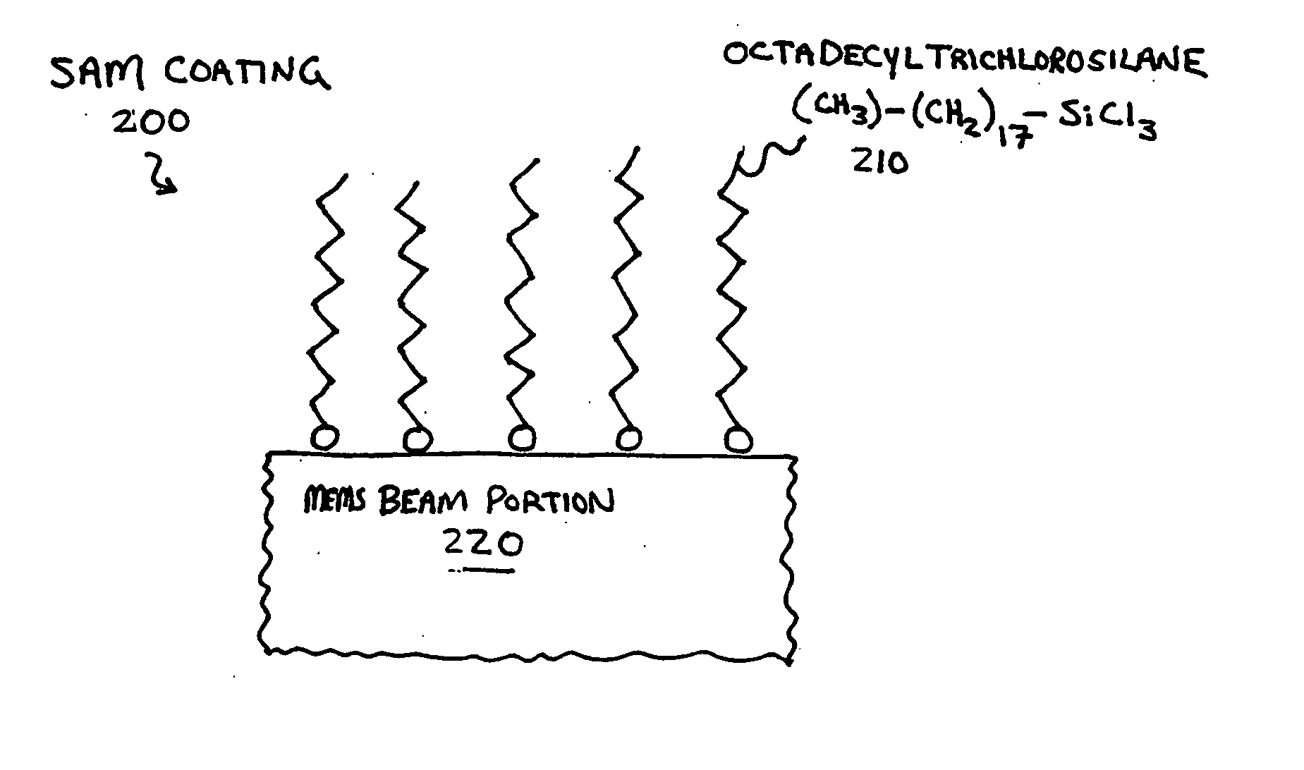
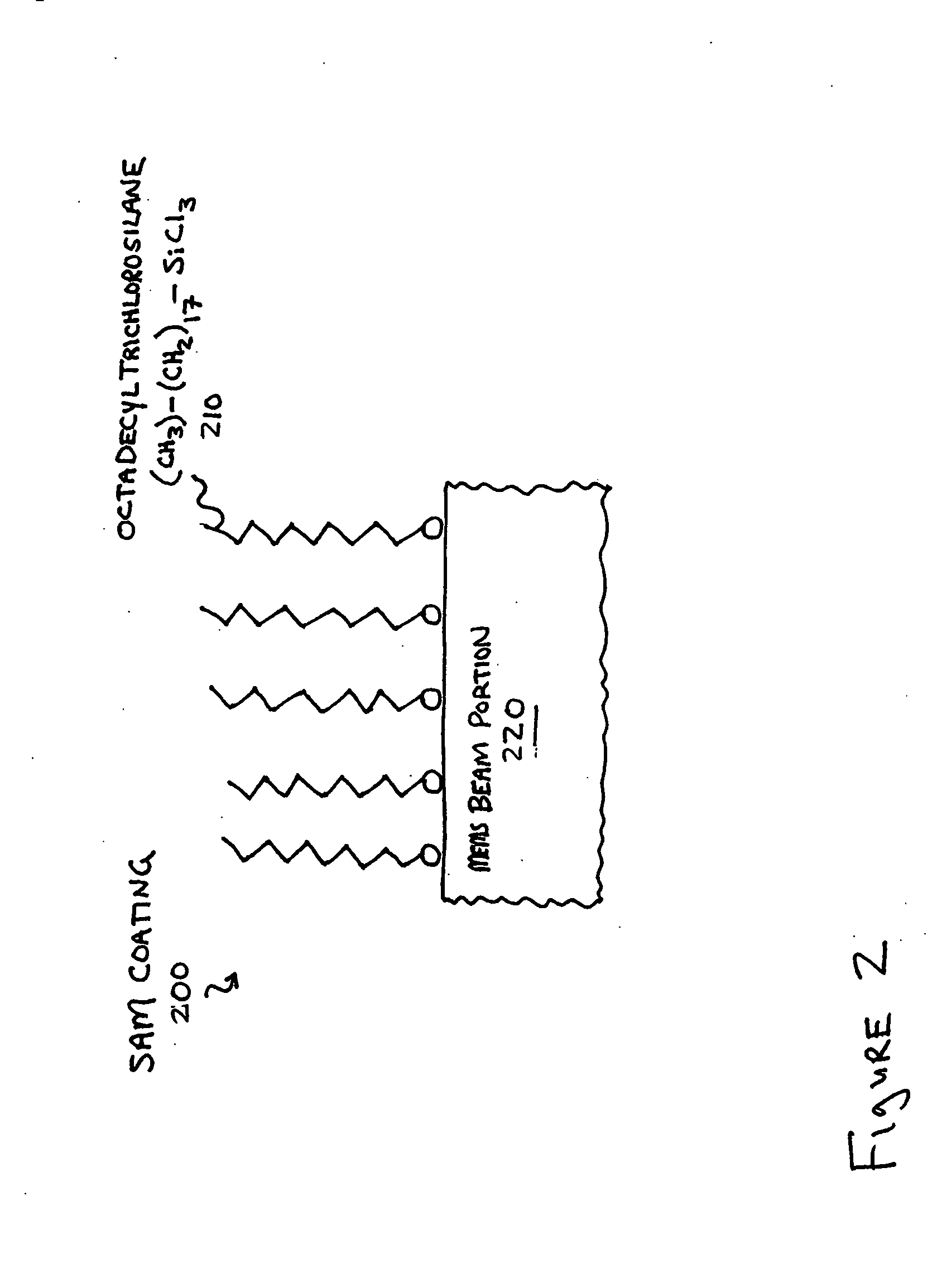
This self-assembled monolayer approach has a number of limitations.
One limitation is that the coatings are organic and have a very limited range of properties.
The organic coatings do not work well for several surfaces commonly used in MEMS.
Another limitation is that the coatings are limited to a single monolayer, and as such do not provide sufficient electrical insulation, or sufficient protection against frictional wear.
However, CVD has several significant limitations that render it generally unsuitable for MEMS.
One limitation is that the high deposition temperatures for CVD are often not suitable for MEMS.
Differences in coefficients of thermal expansion between the deposition layer and underlying materials, over the large temperature range between deposition temperature and ambient, may create significant material stresses between the deposition layer and underlying materials.
Another limitation is that the deposited layers do not have uniform thickness.
Accordingly, prior art methods for depositing layers on MEMS have a number of significant limitations and improved systems and methods for depositing layers on MEMS are needed.

Method used


Image

  • Al2O3 atomic layer deposition to enhance the deposition of hydrophobic or hydrophilic coatings on micro-electromechcanical devices
  • Al2O3 atomic layer deposition to enhance the deposition of hydrophobic or hydrophilic coatings on micro-electromechcanical devices
  • Al2O3 atomic layer deposition to enhance the deposition of hydrophobic or hydrophilic coatings on micro-electromechcanical devices

Examples


example 1

Depositing a Frictional Wear Reducing Layer on a Micro-Mechanical Device

ALD may be used to deposit materials suitable to reduce frictional wear on micro-mechanical devices. This may be achieved by depositing a layer comprising a material having a hardness, wear-resistance, coefficient of friction, or other material characteristic more favorable than that of at least a portion of the device to protect moving parts from frictional wear and increase the life of the device. For example, the device may comprise a first silicon portion having a hardness of about 10-12 GPa (about 7 on the Mohs hardness scale) to contact a second silicon portion having a similar hardness and the deposited layer may comprise a material sufficiently harder than silicon deposited on the first portion and the second portion. Advantageously, the layer may contact on behalf of the first portion and the second portion and may reduce wear due to the greater hardness. For example, the material deposited may compri...

example 2

Depositing an Electrically Insulating Layer on a Micro-Electromechanical Device

ALD may be used to deposit materials suitable to reduce electrical shorting in micro-electromechanical devices. This may be achieved by depositing a layer that comprises a material or materials that have sufficient electrical properties to prevent electrical shorting between proximate electrical components or between proximate devices. This may be done by depositing a material that is sufficiently dielectric (i.e., provides sufficient electrical insulation) or that has a sufficient electrical resistance to prevent electrical shorting.

Consider a micro-mechanical device that has a first silicon portion to contact a second proximate silicon portion. Silicon has particular electrical properties including a dielectric constant of about 11-12 and an electrical resistance of about 1 Ohm*cm for doped silicon. Such electrical properties may lead to an electrical shorting tendency that may be reduced by deposit...

example 3

Exemplary Device Having a Wear Reducing and Electrically Insulating Layer

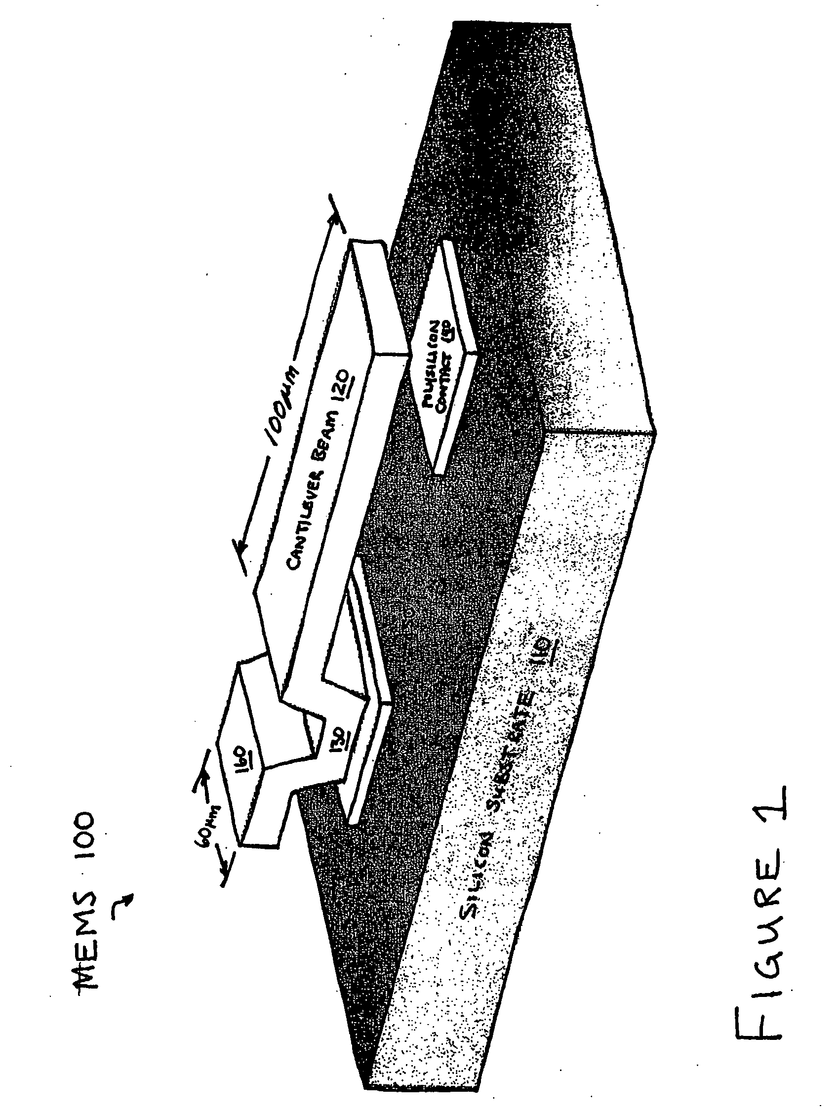
FIG. 13 shows a side view of a cantilever MEMS 1300 having a layer of Al2O3 deposited thereon by ALD. According to one embodiment, the layer may be deposited by the method of FIG. 11. Advantageously, the layer of Al2O3 may be sufficiently hard to reduce frictional wear to the MEMS 1300 and sufficiently dielectric to reduce electrical shorting to the MEMS 1300.

The device 1300 includes a cantilever beam 1320 having a bottom surface 1321 and enclosing a void 1370, a first polysilicon contact plate 1340, an anchor 1330 to fixedly attach the beam 1320 to the plate 1340, a second polysilicon contact plate 1340, a silicon substrate 1310 fixedly attached with the first plate 1340 and the second plate 1350, and a layer of Al2O3 1390 deposited conformally and in substantially uniform thickness to an exposed outer surface of the device 1300 including the bottom surface 1321 and a housing of the void 1370. Advantageousl...


PUM

PropertyMeasurementUnit
Angleaaaaaaaaaa
Angleaaaaaaaaaa
Thicknessaaaaaaaaaa

Abstract

Micro-mechanical devices, such as MEMS, having layers thereon, and methods of forming the layers, are disclosed. In one aspect, a method may include forming a layer including an oxide of aluminum over at least a portion of a micro-mechanical device, and coating the layer by bonding material to surface hydroxyl groups of the layer. In another aspect, a method may include introducing a micro-mechanical device into an atomic layer deposition chamber, and substantially filling nanometer sized voids of the micro-mechanical device by using atomic layer deposition to introduce material into the voids. In a still further aspect, a method may include introducing an alkylaminosilane to a micro-mechanical device having a surface hydroxyl group, and bonding a silane to the micro-mechanical device by reacting the alkylaminosilane with the surface hydroxyl group.

Description

COPYRIGHT NOTICE Contained herein is material that is subject to copyright protection. The copyright owner has no objection to the facsimile reproduction by anyone of the patent document or the patent disclosure, as it appears in the United States Patent and Trademark Office patent file or records, but otherwise reserves all rights to the copyright whatsoever. The following notice applies to the text and data as described below and in the drawings hereto: Copyright© 2001, University of Colorado Technology Transfer Office, All Rights Reserved. BACKGROUND OF THE INVENTION 1. Field of the Invention The invention relates generally to micro-mechanical devices. 2. Background Information MicroElectroMechanical Systems (MEMS) are miniature devices that combine micro-electronics with micro-mechanics. The MEMS, which typically have a size ranging from less than a millimeter (m, one thousandth of a meter) to more than about a micrometer (μm, one millionth of a meter), may be used individu...

Claims


Application Information

Patent Timeline
IPC IPC(8): B81B3/00B81C1/00G02B26/08
CPCB81B3/0005B81C1/0096G02B26/0866B82Y30/00G02B26/0833B81C2201/112
Inventor GEORGE, STEVEN M.HERRMANN, CARI F.
Owner UNIV OF COLORADO THE REGENTS OF
Learn More