Post-passivation metal scheme on an IC chip with copper interconnection

Inactive Publication Date: 2005-01-27
QUALCOMM INC
View PDF14 Cites 85 Cited by
  • Summary
  • Abstract
  • Description
  • Claims
  • Application Information

AI Technical Summary

Benefits of technology

[0018] Also in accordance with the objects of the invention, a method

Problems solved by technology

However, copper interconnection also incurs reliability concerns.
When a copper I/O pad is exposed to atmosphere, its surface is subjected to chemical attack by the oxygen and moisture in the atmosphere.
One of the major challenges in the creation of analog processing circuitry (using digital processing procedures and equipment) is that a number of the components that are used for analog circuitry are large in size and are therefore not readily integrated into devices that typically have feature sizes that

Method used


Image

  • Post-passivation metal scheme on an IC chip with copper interconnection
  • Post-passivation metal scheme on an IC chip with copper interconnection
  • Post-passivation metal scheme on an IC chip with copper interconnection

Examples


Example

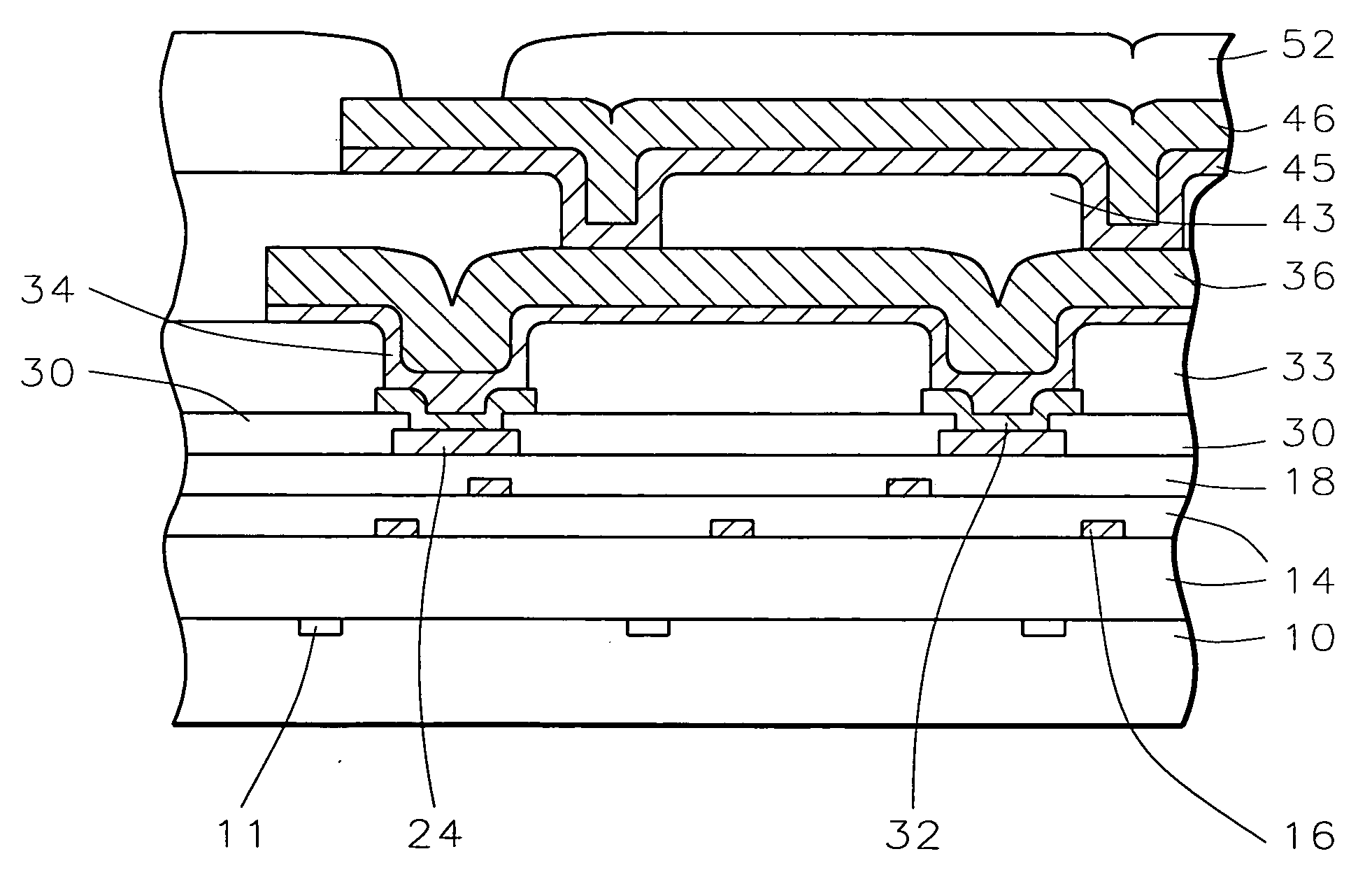
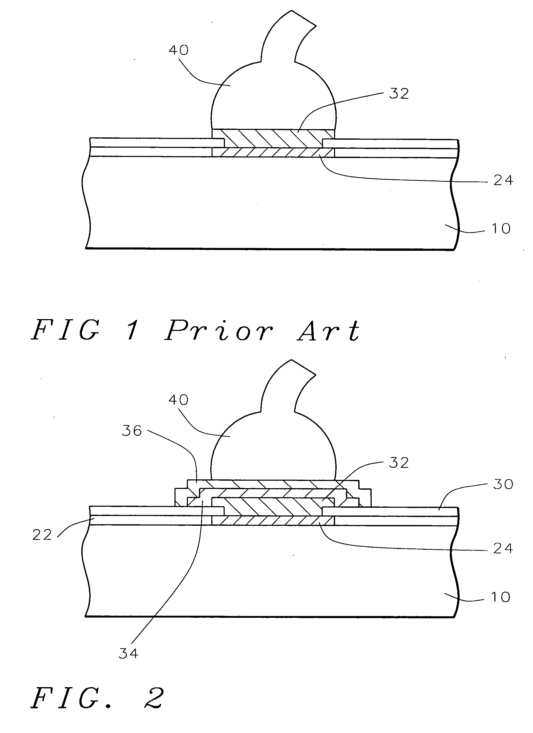
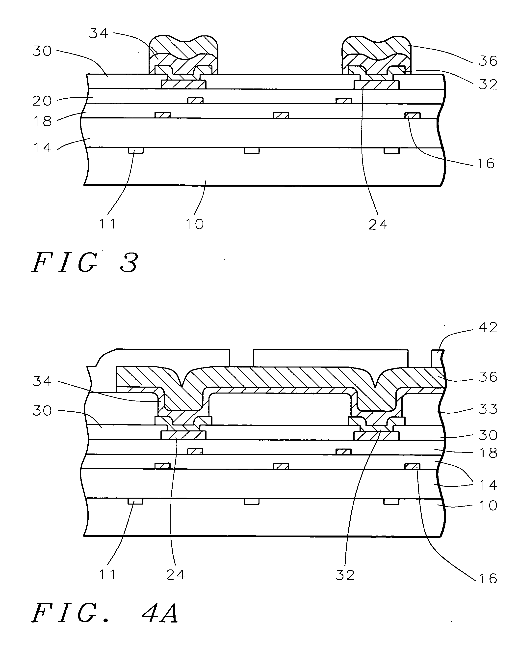
[0028] The prior art did not extend the application of a metal cap layer to other useful applications such as post-passivation interconnection or testing through the redistribution layer (RDL). The present invention discloses a structure and method to extend the concept of a metal cap on a copper interconnection to a post-passivation interconnection scheme. In a post passivation processing sequence, as described in copending U.S. patent application Ser. No. 10 / 154662 filed on May 24, 2002 and herein incorporated by reference, a thick layer of dielectric is optionally deposited over a layer of passivation and layers of wide and thick metal lines are formed on top of the thick layer of dielectric.

[0029] By adding a post-passivation interconnection scheme on a metal (such as Al) pad, where the post-passivation metal is, for example, gold or copper, several advantages emerge. A post-passivation metal trace can be formed either as a stripe or a meander line. When the trace is formed as ...


PUM


Abstract

In the present invention, copper interconnection with metal caps is extended to the post-passivation interconnection process. Metal caps may be aluminum. A gold pad may be formed on the metal caps to allow wire bonding and testing applications. Various post-passivation passive components may be formed on the integrated circuit and connected via the metal caps.

Description

[0001] This application claims priority to U.S. Provisional Patent Application Ser. No. 60 / 489564, filed on Jul. 23, 2003, which is herein incorporated by reference.RELATED PATENT APPLICATIONS [0002] This application is related to attorney docket number MS98-002CCC-CIP, Ser. No. 10 / 154662, filed on May 24, 2002, and assigned to a common assignee. [0003] This application is related to attorney docket number MEG02-016, Ser. No. 10 / 445558, filed on May 27, 2003, and assigned to a common assignee. [0004] This application is related to attorney docket number MEG02-017, Ser. No. 10 / 445559, filed on May 27, 2003, and assigned to a common assignee. [0005] This application is related to attorney docket number MEG02-018, Ser. No. 10 / 445560, filed on May 27, 2003, and assigned to a common assignee. BACKGROUND OF THE INVENTION [0006] 1. Field of the Invention [0007] This invention relates to structures and methods of assembly of integrated circuit chips. More particularly, this invention relate...

Claims


Application Information

Patent Timeline
IPC IPC(8): H01L23/485H01L23/522H01L23/532
CPCH01L23/5222H01L23/53238H01L23/53252H01L24/05H01L24/45H01L24/48H01L2224/04042H01L2224/05083H01L2224/05124H01L2224/05147H01L2224/05157H01L2224/05166H01L2224/05171H01L2224/05181H01L2224/05184H01L2224/05187H01L2224/05624H01L2224/05644H01L2224/05647H01L2224/45144H01L2224/48463H01L2224/48624H01L2224/48644H01L2224/48647H01L2924/01011H01L2924/01013H01L2924/01014H01L2924/01022H01L2924/01027H01L2924/01028H01L2924/01029H01L2924/01047H01L2924/0105H01L2924/01073H01L2924/01074H01L2924/01079H01L2924/01327H01L2924/014H01L2924/04941H01L2924/04953H01L2924/05042H01L2924/14H01L2924/19041H01L2924/19042H01L2924/19043H01L2924/30105H01L2924/01019H01L2924/01024H01L2924/01033H01L2924/00014H01L2924/00
Inventor LIN, MOU-SHIUNGCHEN, MICHAELCHOU, CHIEN KANGCHOU, MARK
Owner QUALCOMM INC
Why Eureka
Try Eureka