
Photoresist stripping solution and a method of stripping photoresists using the same

a technology of photoresist and stripping solution, which is applied in the direction of photomechanical equipment, instruments, photosensitive material processing, etc., can solve the problems of reducing the yield of semiconductor fabrication, affecting the performance of the substrate, and unable to provide adequate protection against corrosion of the substrate, so as to achieve the effect of protecting al

Inactive Publication Date: 2005-01-27
WAKIYA KAZUMASA +1
View PDF4 Cites 3 Cited by
  • Summary
  • Abstract
  • Description
  • Claims
  • Application Information

AI Technical Summary

Benefits of technology

The present invention has been accomplished under these circumstances and has as an object of providing a photoresist stripping solution that is suitable for use in the photolithographic technology to form today's semiconductor and liquid-crystal display devices having an ever decreasing feature size and an increasing number of interlevel films superposed on the substrate, and that can assure effective protection of Al, Cu and other wiring metal conductors against corrosion as well as efficient stripping of the photoresist film, post-ashing residues and metal depositions.

Problems solved by technology

A problem with this approach is that wiring delay is caused by the resistance of the metal films used (wiring resistance) and wiring capacity.
Unless the Cu and Si depositions are completely stripped away, problems will occur such as lower yield of semiconductor fabrication.
A problem with the stripping solutions proposed in those patents is that if their ability to strip the photoresist film and post-ashing residues, particularly the ability to strip Si-based residues, is enhanced to an adequate level, they are not capable of providing adequate protection against corrosion of the Si substrate, particularly its reverse side; hence, the ability to strip the Si-based residues must be compromised to some extent.
However, for successful lithography in today's practice of fabricating semiconductor devices with an ever decreasing feature size and an increasing number of interlevel films superposed on the substrate, stripping of the Si-based residues cannot be compromised and it is desired to develop a stripping solution that meets both requirements for efficient stripping of Si-based residues and effective protection of the Si substrate from corroding.
A group of stripping solutions that contain hydroxylamines have also been proposed, but the starting materials from which they are made are highly hazardous (e.g. explosive) and at the stage of purification, they are not easy to handle since they are toxic or hazardous.

Method used


Image

  • Photoresist stripping solution and a method of stripping photoresists using the same
  • Photoresist stripping solution and a method of stripping photoresists using the same
  • Photoresist stripping solution and a method of stripping photoresists using the same

Examples


examples

The following examples are provided for the purpose of further illustrating the present invention but are in no way to be taken as limiting. Unless otherwise noted, all compounding amounts are expressed by mass percent.

examples 13-19

[Substrate I]

Processed substrates were prepared by repeating the procedure employed in Examples 1-12.

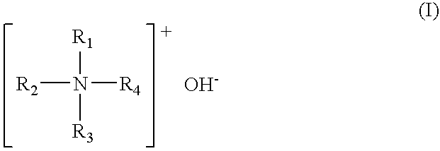
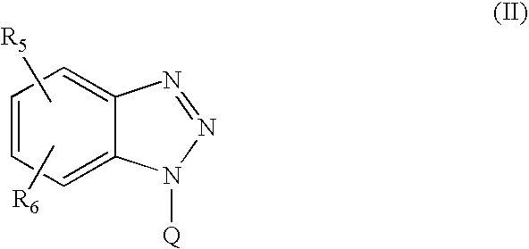
The processed substrates were stripped away of the post-ashing residues by dipping in photoresist stripping solutions (70° C.×30 min) consisting of 5 mass percent of tetrapropylammonium hydroxide (TPAH) as component (a), 20 mass percent of monoethanolamine (MEA) as component (b), 40 mass percent of component (c), and 30 mass percent of N-methyl-2-pyrrolidone (NMP) as component (e), plus 5 mass percent of component (d) (see Table 4 for the specific compound used), followed by rinsing with pure water. The strippability of the Al-based residue formed on the sidewall of each hole, the strippability of the Si-based residue formed around the opening of each hole, the state of corrosion of the Al wiring at the bottom of each hole, and the state of corrosion of Si in the reverse surface of the silicon wafer were evaluated by examination with an SEM (scanning electron microscope). The res...


PUM


Abstract

A photoresist stripping solution comprising (a) a specified quaternary ammonium hydroxide, such as tetrabutylammonium hydroxide, tetrapropylammonium hydroxide, methyltributylammonium hydroxide or methyltripropylammonium hydroxide, (b) a water-soluble amine, (c) water, (d) a corrosion inhibitor and (e) a water-soluble organic solvent, the compounding ratio of component (a) to component (b) being in the range of from 1:3 to 1:10 by mass, as well as a method of stripping photoresists using the solution. The stripping solution of the invention assures effective protection of Al, Cu and other wiring metal conductors against corroding as well as efficient stripping of the photoresist film, post-ashing residues such as modified photoresist film and metal depositions. It also assures efficient stripping of Si-based residues and effective protection of the substrate (particularly the reverse side of a Si substrate) from corroding.

Description

This application is a continuation of U.S. patent application Ser. No. 10 / 208,054, filed Jul. 31, 2002, now abandoned. BACKGROUND OF THE INVENTION 1. Field of the Invention This invention relates to a photoresist stripping solution and a method of stripping photoresists using the same. The invention is suitable for use in the fabrication of semiconductor devices such as ICs and LSIs, as well as liquid-crystal panel apparatus. 2. Description of Relevant Art The fabrication of semiconductor devices such as ICs and LSIs, as well as liquid-crystal panel apparatus, comprises forming a uniform photoresist coating over conductive metallic layers, insulation layers such as an SiO2 film formed on a substrate (silicon wafer) by CVD; performing selective exposure and development to form a photoresist pattern; selectively etching the substrate having the conductive metallic layers, the insulation layers formed thereon by CVD, using the photoresist pattern as a mask to thereby form a microc...

Claims


Application Information

Patent Timeline
IPC IPC(8): C11D1/62C11D7/32C11D11/00G03F7/42
CPCC11D1/62C11D7/32H01L21/02068G03F7/425G03F7/426C11D11/0047C11D2111/22
Inventor WAKIYA, KAZUMASAYOKOI, SHIGERU
Owner WAKIYA KAZUMASA
Learn More