High density chip carrier with integrated passive devices
a chip carrier and passive device technology, applied in the field of high density chip carrier with integrated passive device, can solve the problems of increasing the number of switching events, exacerbate the problem, and the parasitic inductance of the currently used discrete capacitor is not sufficiently low to be used, and achieves low inductance, low resistance integration, and fast electrical access
- Summary
- Abstract
- Description
- Claims
- Application Information
AI Technical Summary
Benefits of technology
Problems solved by technology
Method used
Image
Examples
first embodiment
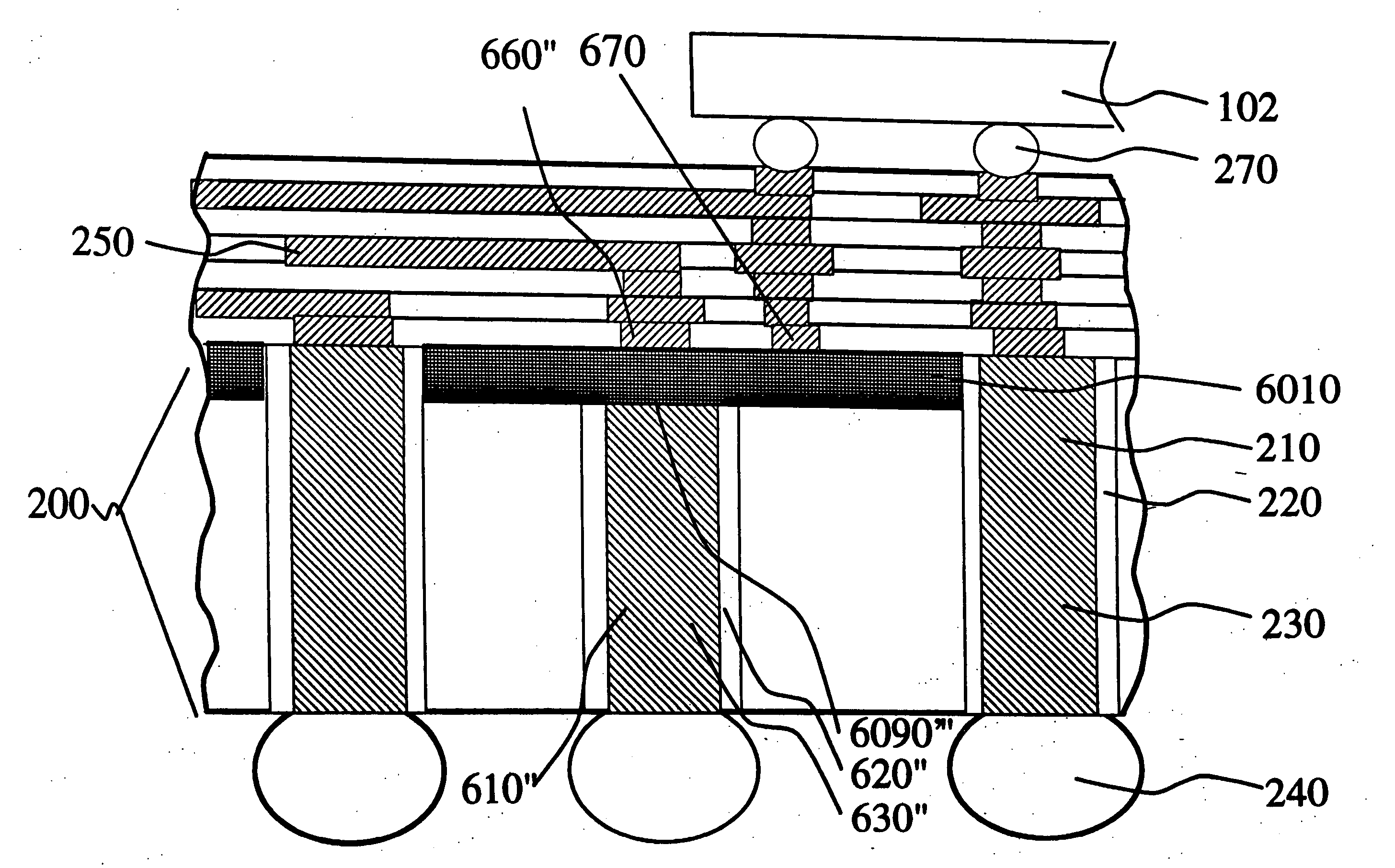
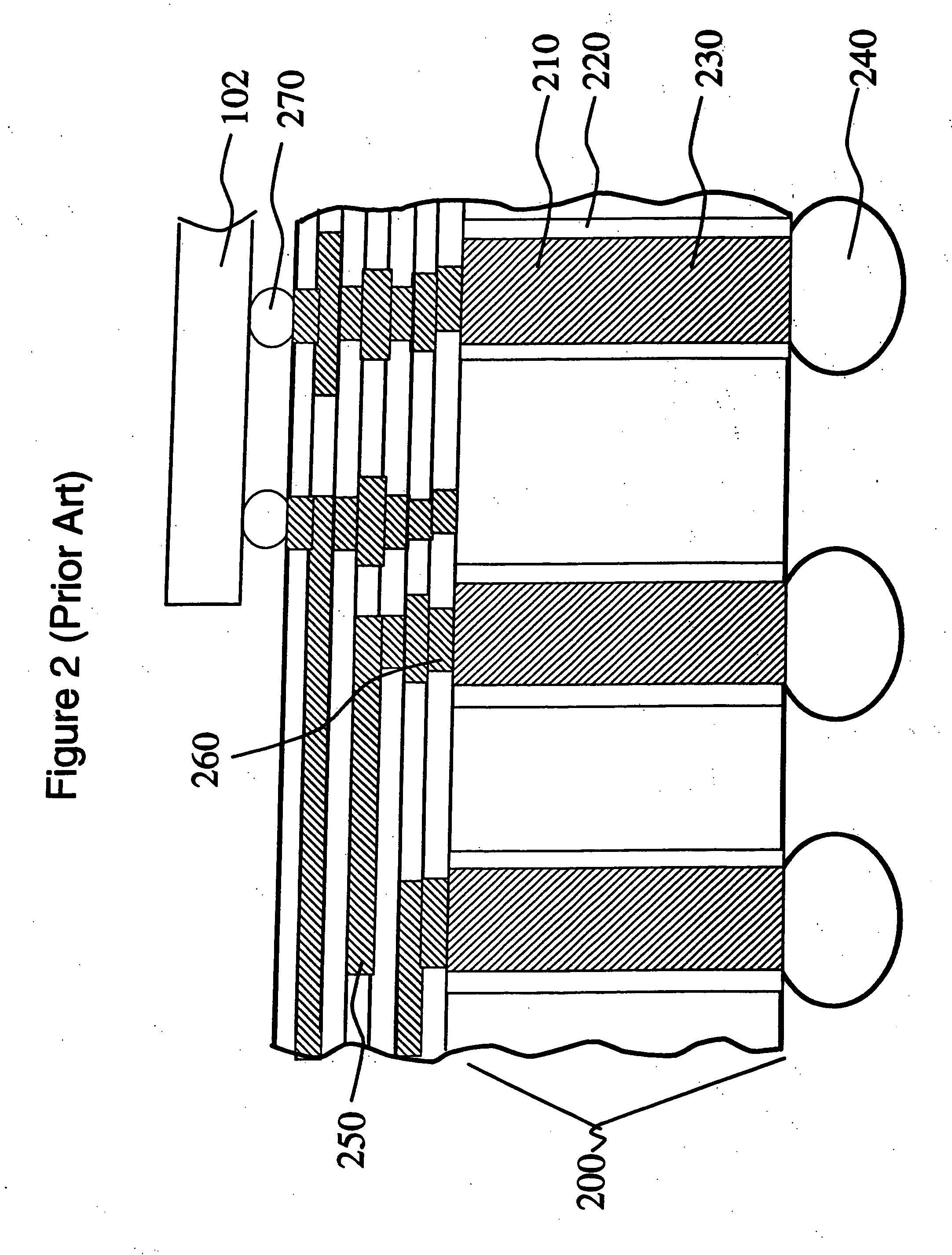
[0029] our inventive design enhances the prior art silicon carrier by adding integrated decoupling capacitors and allowing these passive elements to be accessed by the chips mounted on the carrier through the micro joint I / O connections. The decoupling capacitor arrays in the form of deep trench capacitors are built on the top surface region of the silicon carrier which is not already occupied by the through via features. FIG. 3a shows the schematic representation of such a structure. This embodiment comprises all the prior art features depicted in FIG. 2, but additionally comprises deep trench decoupling capacitor structures 3010 formed adjacent to the silicon through vias 210. State of the art processing used in the fabrication of these deep trenches 3010, such as lithography and reactive ion etching, allows for up to 40:1 aspect ratio, which means that trenches are 40 times as deep as they are wide. The trenches used in the process of this invention have widths between 100 nm and...
second embodiment
[0032] In a second embodiment, the second trench capacitor option designated as metal-insulator-silicon (MIS) depicted schematically in FIG. 3c is used. As in the case of the MIM option of FIG. 3b, the MIS trench capacitors of FIG. 3c are also situated on the top surface of the silicon carrier in the spaces between the through vias. In the MIS option, after the trenches 3010 are formed, an implantation and anneal step is performed to render the trench surfaces and tops highly conductive creating a heavily doped “well” region 3080′. This well 3080′ acts as the bottom electrode in this structure. The dopants are implanted with a doping concentration in the range of 10−18 to 10−21 atoms / cm2 to achieve low resistivity (<0.01 ohm-cm). The depth of the doping region may vary in the range of 50 nm to 500 nm. Dopants that can be used in forming the bottom conductive layer may be As, P, B and combinations thereof.
[0033] The rest of the process flow is identical to the MIM process flow except...
PUM
 Abstract
Description
Claims
Application Information


