

Curable encapsulant compositions
a technology of encapsulant composition and composition, which is applied in the direction of semiconductor/solid-state device details, instruments, photosensitive materials, etc., can solve the problems of affecting the overall electronic device and/or substrate, and affecting the quality of encapsulant,
- Summary
- Abstract
- Description
- Claims
- Application Information
AI Technical Summary
Benefits of technology
Problems solved by technology
Method used
Image

Examples
example 1
Cycloaliphatic resin (Union Carbide, UVR 6128), 55.2%, pre-oligomerised CER (CAT002, UCB), 33.68%, organosilane (Silquest 187, OSI) 2.0%, fumed silica, 2.5%, iodonium salt photo-initiator, 2.5%, isopropyl thiaxanthone, 0.02%, “Blue 50” (Spectra Group Limited) 2.0%, were blended together and deaerated in the absence of light.
The resulting mixture was a straw yellow transparent liquid.
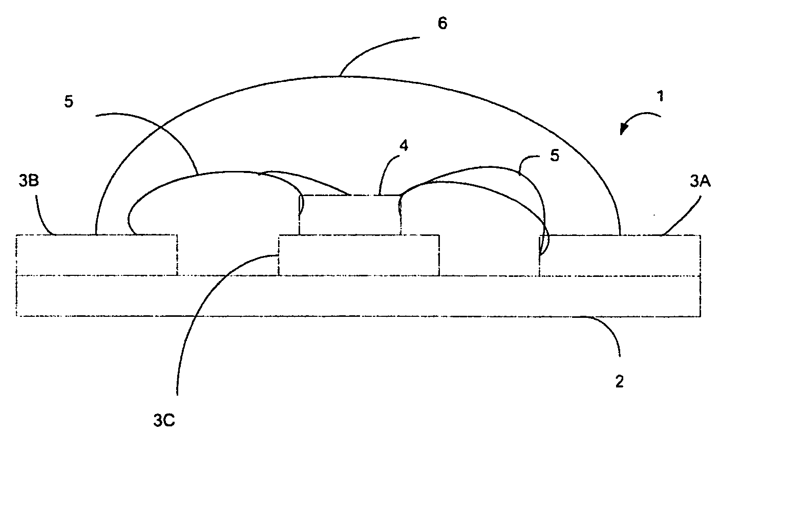
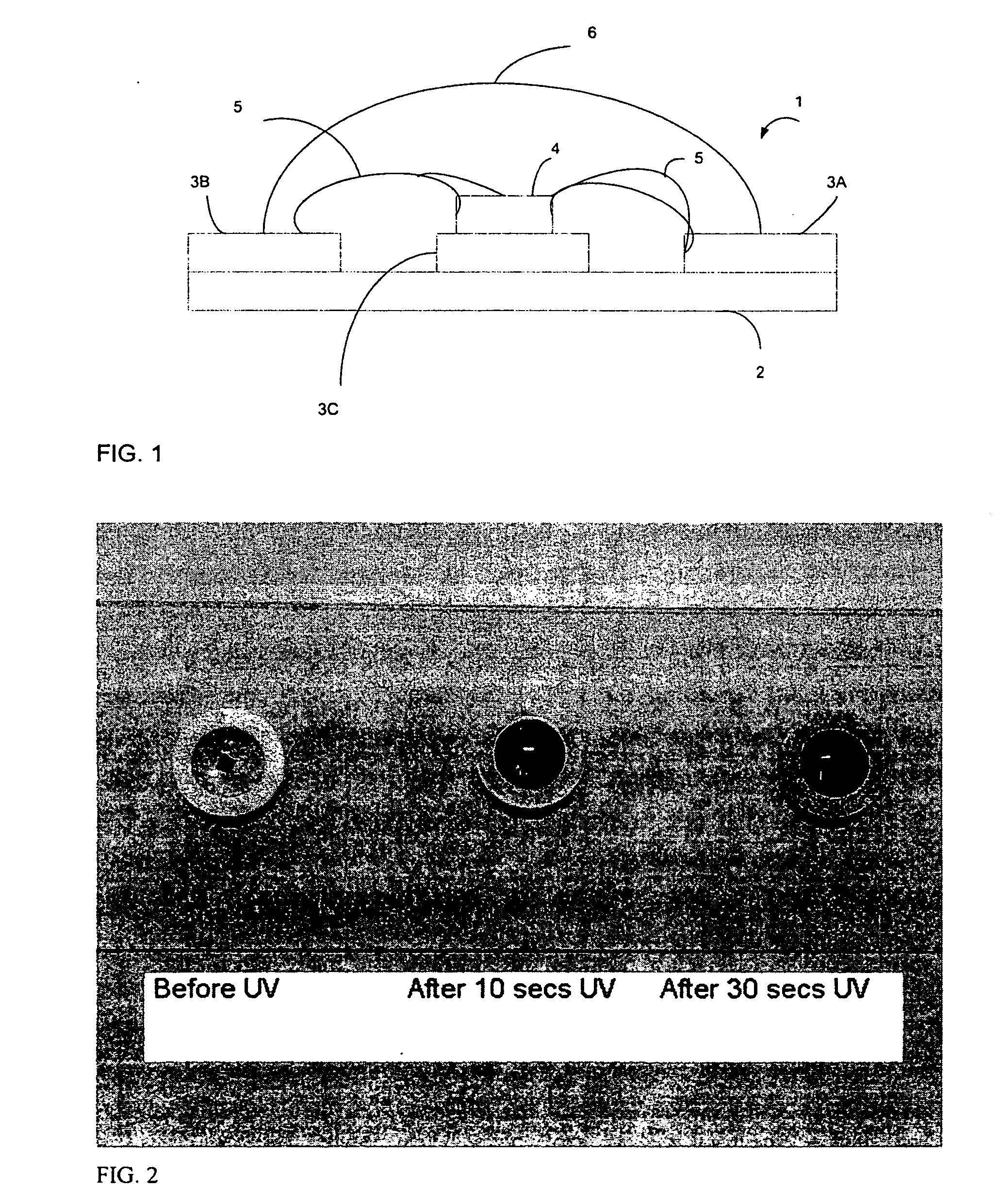
Approximately 200 mg of this mixture was dispensed onto a glass slide so as to encapsulate a chip / die on the slide. The composition was cured with uv light with an intensity of 100 mW / cm2 for 30 seconds.
The resulting cured material was solid and opaque and dark blue / black in colour. A CTV measurement of this formulation cured with uv light with an intensity of 100 mW / cm2 for 30 seconds showed an average cure depth of 1600 microns. FIG. 2 shows the precure and 10 and 30 second cure product of the composition which has been dispensed for use as an encapsulant on the chip / die.
example 2
Another formulation was prepared which incorporated a further opacifying component.
Cycloaliphatic resin (Union Carbide, UVR 6128), 55.1%, pre-oligomerised CER (CAT002, UCB), 33.68%, organosilane (Silquest 187, OSI) 2.0%, fumed silica, 2.5%, iodonium salt photo-initiator, 2.5%, isopropyl thiaxanthone, 0.02%, micronised carbon black, 0.1%, “Blue 50” (Spectra Group Limited) 2.0%, were blended together and deaerated in the absence of light.
The resulting mixture was a straw yellow transparent liquid with black particulate suspension.
Approximately 200 mg of the mixture was dispensed onto a glass slide so as to encapsulate a chip / die on the slide. The composition was cured with uv light with an intensity of 100 mW / cm2 for 30 seconds.
The resulting cured material was solid and opaque and is black in colour. A cure through volume measurement of this formulation cured with uv light with an intensity of 100 mW / cm2 for 30 seconds showed an average cure depth of 1000 microns.
example 3
Another formulation of the present invention was prepared in which isopropyl thiaxanthone was replaced by Hu470.
Cycloaliphatic resin (Union Carbide, UVR 6128), 55.1%, pre-oligomerised CER (CAT002, UCB), 33.68%, organosilane (Silquest 187, OSI) 2.0%, fumed silica, 2.5%, iodonium salt photoinitiator, 2.5%, photosensitizer (Spectra Group Limited Hu470) 0.25%, “Blue 50” (Spectra Group Limited) 2.0%, were blended together and deaerated in the absence of light.
The resulting mixture was a straw yellow transparent liquid.
Approximately 200 mg of this mixture was dispensed onto a glass slide so as to encapsulate a chip / die on the glass slide. The composition was then cured with uv light with an intensity of 100 mW / cm2 for 30 seconds.
The resulting cured material was solid and opaque and black in colour. A cure through volume measurement of this formulation cured with uv light with an intensity of 100 mW / cm2 for 30 seconds showed an average cure depth of 1800 microns.
PUM
| Property | Measurement | Unit |
|---|---|---|
| Temperature | aaaaa | aaaaa |
| Temperature | aaaaa | aaaaa |
| Percent by mass | aaaaa | aaaaa |
Abstract
Description
Claims
Application Information