Method for writing data to a semiconductor memory comprising a peripheral circuit section and a memory core section including a memory cell

a technology of semiconductor memory and peripheral circuit, which is applied in the direction of information storage, static storage, digital storage, etc., can solve the problems of inability to greatly reduce the cycle time (random cycle time=trc) of the memory core, and the difficulty of making random access to cell data in the memory core, so as to reduce the random cycle time and reduce the data path

Inactive Publication Date: 2005-02-03
KK TOSHIBA
View PDF4 Cites 9 Cited by
  • Summary
  • Abstract
  • Description
  • Claims
  • Application Information

AI Technical Summary

Benefits of technology

[0009] Accordingly, an object of this invention is to provide a semiconductor memory device capable of reducing random cycle time

Problems solved by technology

In order to enhance the data transfer rate in the SDRAM, the data bandwidth is actively increased, but it is difficult to make random access to cell data in a memory core, that is, to enhance the speed of data access to a row address which has been changed to indicate a different row.
This is because the cycle ti

Method used


Image

  • Method for writing data to a semiconductor memory comprising a peripheral circuit section and a memory core section including a memory cell
  • Method for writing data to a semiconductor memory comprising a peripheral circuit section and a memory core section including a memory cell
  • Method for writing data to a semiconductor memory comprising a peripheral circuit section and a memory core section including a memory cell

Examples


first embodiment

[0034] [First Embodiment]

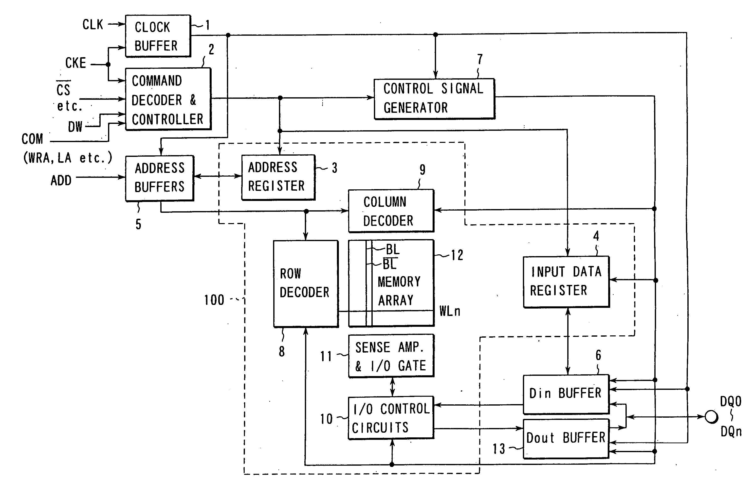
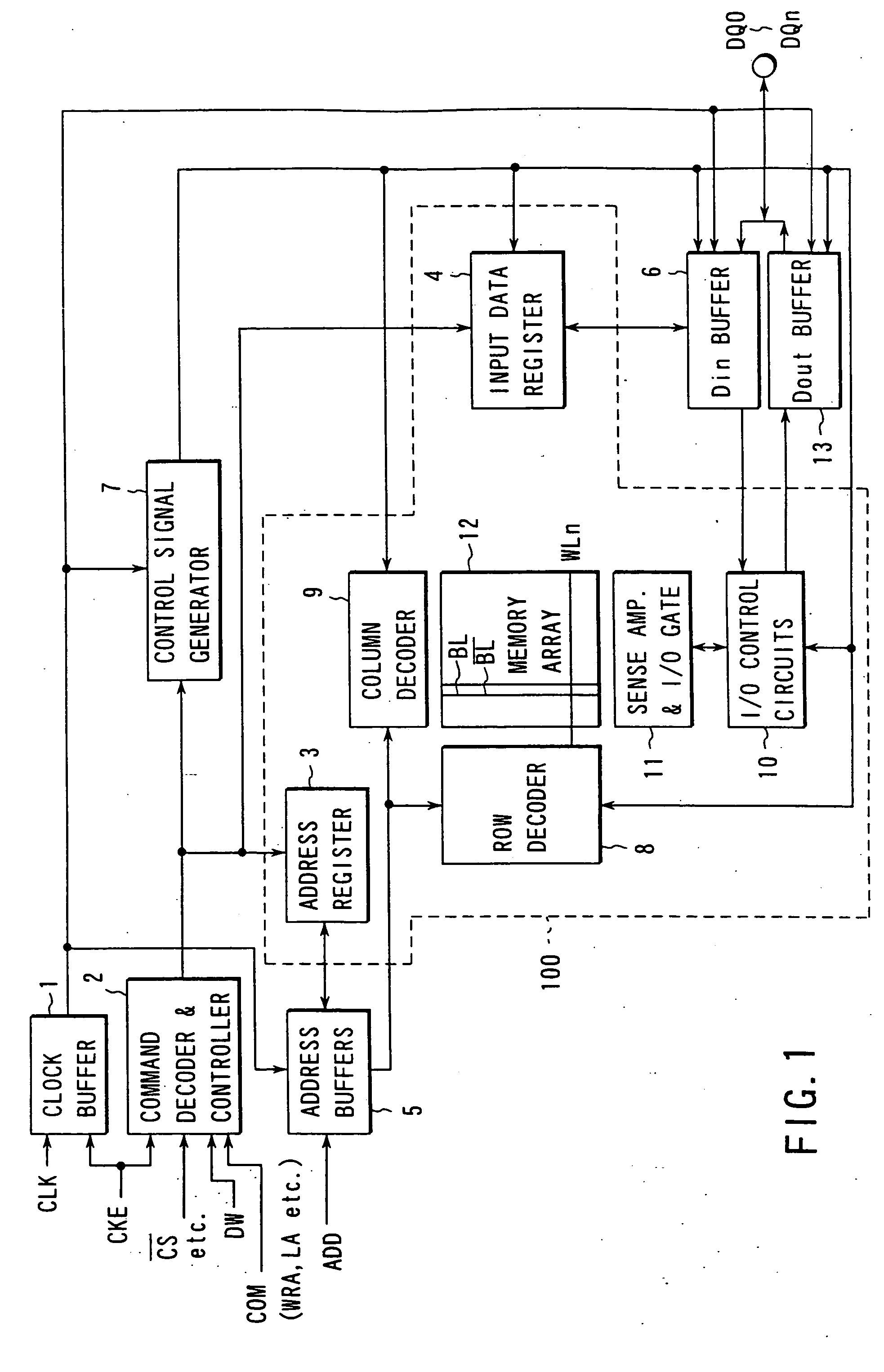
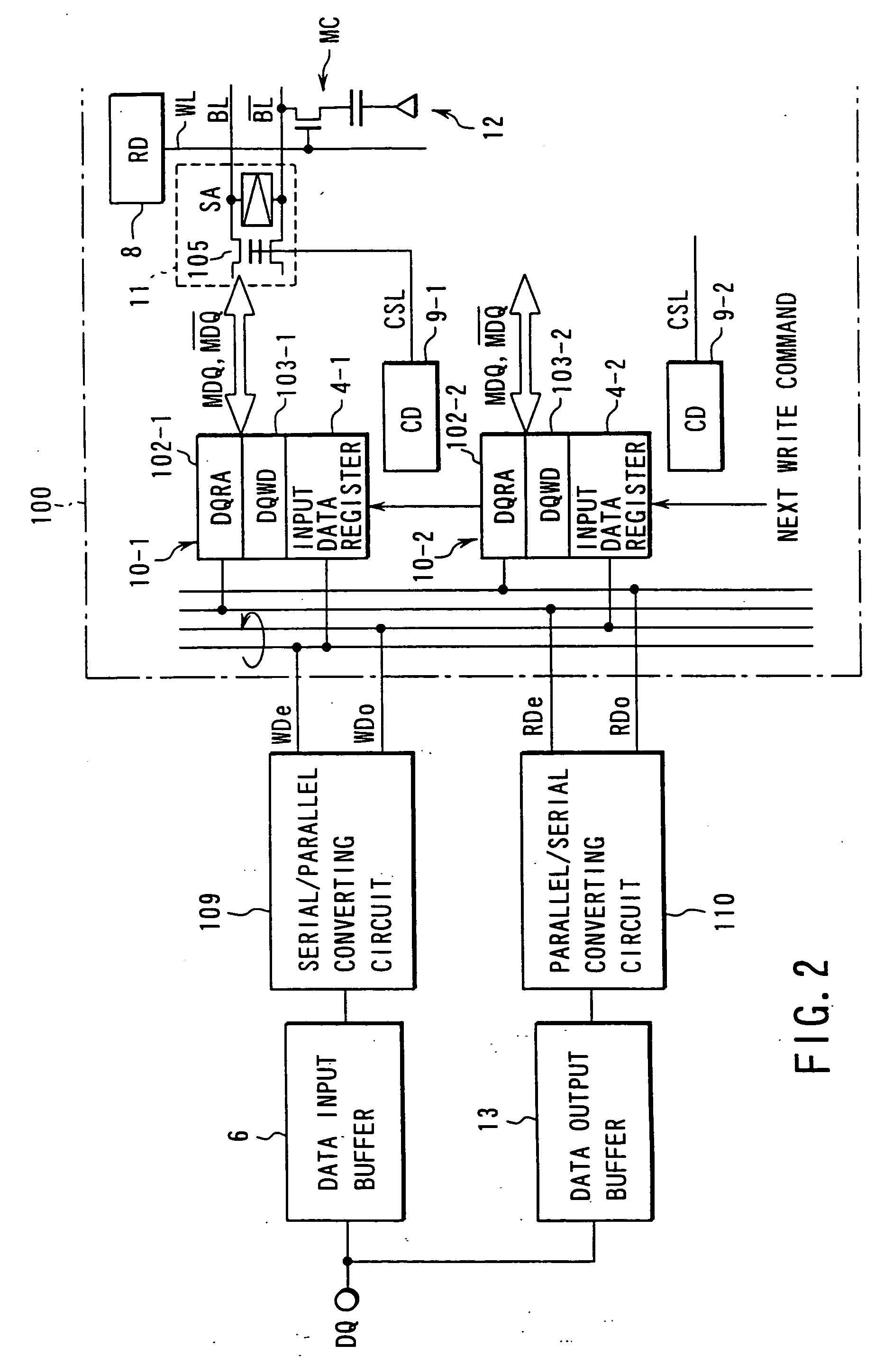
[0035] FIGS. 1 to 4 are diagrams for illustrating a semiconductor memory device according to a first embodiment of this invention, FIG. 1 being a block diagram showing the schematic basic construction of an FCRAM and FIG. 2 being a block diagram showing the schematic construction of an extracted main portion associated with the data write and readout operation of a DDR-SDRAM. Further, FIG. 3 is a circuit diagram showing an example of the concrete circuit construction of a DQ write driver and input data register (latch circuit) in the circuit shown in FIG. 2. FIG. 4 is a timing chart for illustrating the operation of the circuits shown in FIGS. 2 and 3, and in this case, an example in which the burst length is set to “2” based on the specification of the DDR-SDRAM is shown.

[0036] As shown in FIG. 1, the FCRAM (SDR-FCRAM, DDR-FCRAM) includes a clock buffer 1, command decoder & controller 2, address register 3, input data register 4, address buffer 5, data inp...

second embodiment

[0061] [Second Embodiment]

[0062]FIG. 5 is a timing chart for illustrating a data write method for a semiconductor memory device according to a second embodiment of this invention. In the first embodiment, the FCRAM in which the command is supplied in one clock cycle is explained as an example, but the second embodiment is applied to a case wherein the command is supplied as a packet in two successive clock cycles as is disclosed in International Application WO98 / 56004.

[0063] As the actual FCRAM operation, the refresh operation and a function of mode set cycle as in an SDRAM are provided in addition to the read / write operation, and therefore, it is difficult to realize all of the operations by giving a command only once in the random cycle time tRC as explained so far. Therefore, it is more realistic to define the operations by a combination of two commands given as a packet in the successive clock cycles as disclosed in the above Application.

[0064] For example, if a write command ...

third embodiment

[0066] [Third Embodiment]

[0067] FIGS. 6 to 9 illustrate a semiconductor memory device according to a third embodiment of this invention and FIG. 6 is a block diagram showing the schematic basic construction of an FCRAM. FIGS. 7A and 7B are block diagrams each showing the construction of an address coherency detector in the circuit shown in FIG. 6. FIG. 8 is a block diagram showing the schematic construction of an extracted portion associated with the data write and readout operation of a DDR-SDRAM and FIG. 9 is a circuit diagram showing an example of the construction of a readout data switching circuit for switching an output signal of a DQ read amplifier and an output signal of a data register in the circuit shown in FIG. 8.

[0068] The third embodiment is so constructed that data from the input data register 4 is directly read out instead of data from the memory cell when a read command is given before a next write command is given in the late write operation and if it coincides wi...


PUM


Abstract

An input data register for latching write data is arranged in a position near a memory cell array of a memory core section. The input data register is arranged on the upstream side of a data path used for writing data into a memory cell. Write data input to a data pin which is arranged in the end position on the downstream side is latched in the input data register via a data input buffer, serial/parallel converting circuit and write data line. Data latched in the input data register is written into a memory cell via a DQ write driver, data line pair, I/O gate and bit line pair in a next write cycle.

Description

CROSS-REFERENCE TO RELATED APPLICATIONS [0001] This application is based upon and claims the benefit of priority from the prior Japanese Patent Application No. 11-353172, filed Dec. 13, 1999, the entire contents of which are incorporated herein by reference. BACKGROUND OF THE INVENTION [0002] This invention relates to a semiconductor memory device and more particularly to a fast cycle synchronous DRAM (SDR-FCRAM) having a function of rapidly reading / writing random data from or into a memory cell array and a data write system of a double data rate synchronous DRAM (DDR-FCRAM) for realizing the data transfer rate twice that of the above DRAM. [0003] In order to enhance the data access speed of the DRAM-to that of an SDRAM and attain a large data band width (the number of data bytes for each unit time) by use of a high clock frequency (tCK), a synchronous DRAM (SDRAM) is invented and is already put into practice from the 4-Mbit or 16-Mbit DRAM generation. In the present 64-Mbit generat...

Claims


Application Information

Patent Timeline
IPC IPC(8): G11C11/407G11C7/10G11C11/4076G11C11/409
CPCG11C7/1039G11C7/1051G11C7/1069G11C2207/107G11C7/1096G11C11/4076G11C7/1078G11C11/407
Inventor OHSHIMA, SHIGEOOHTAKE, HIROYUKIABE, KATSUMI
Owner KK TOSHIBA
Why Eureka
Try Eureka