

Semiconductor device structural body and electronic device
a technology of semiconductor devices and electronic devices, applied in the direction of semiconductor/solid-state device details, sustainable manufacturing/processing, final product manufacturing, etc., can solve the problems of dislocation of chip parts and inability to correspond to the above-mentioned pb
- Summary
- Abstract
- Description
- Claims
- Application Information
AI Technical Summary
Benefits of technology
Problems solved by technology
Method used
Image

Examples
embodiment 1
[0057] (Embodiment 1)
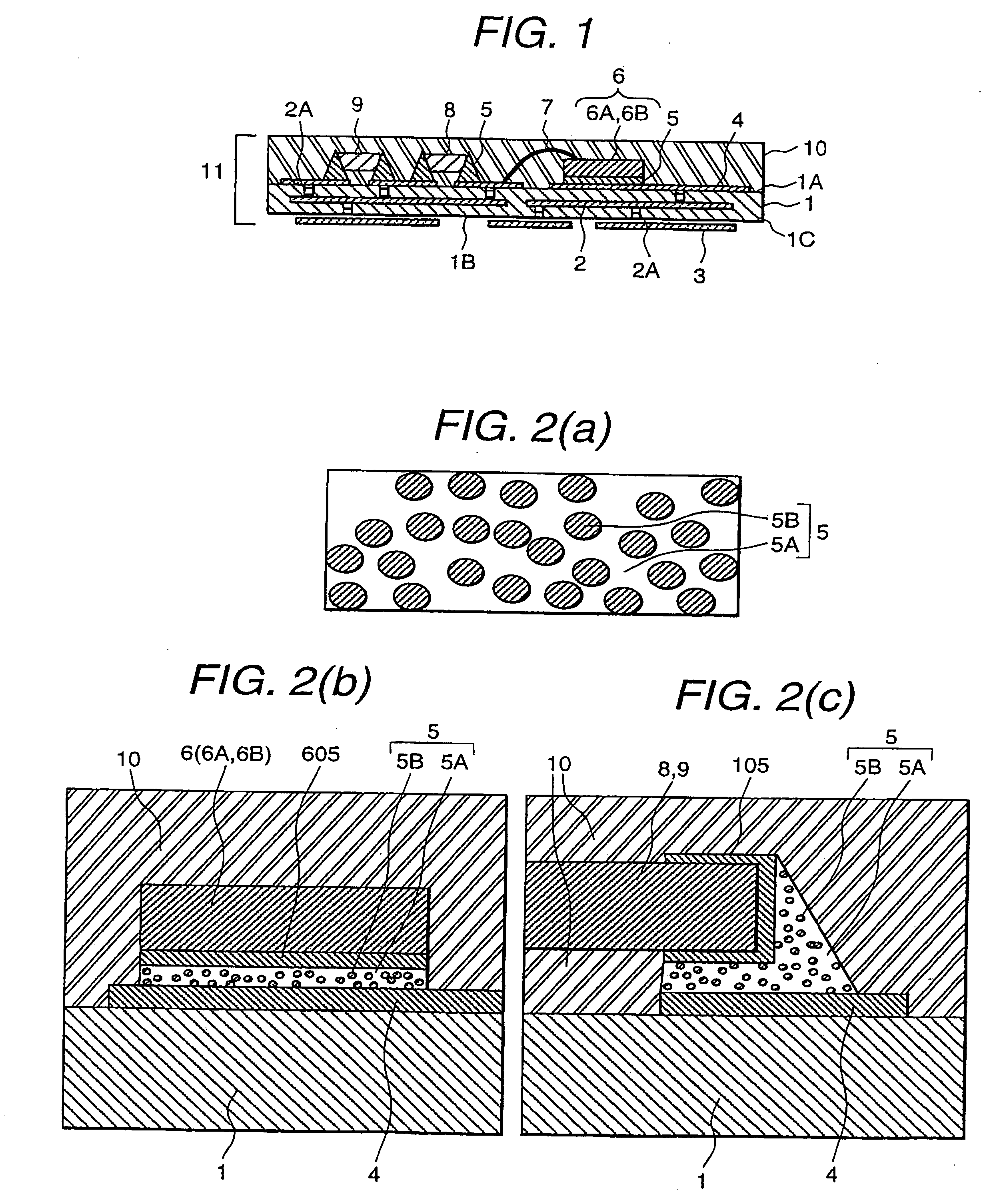
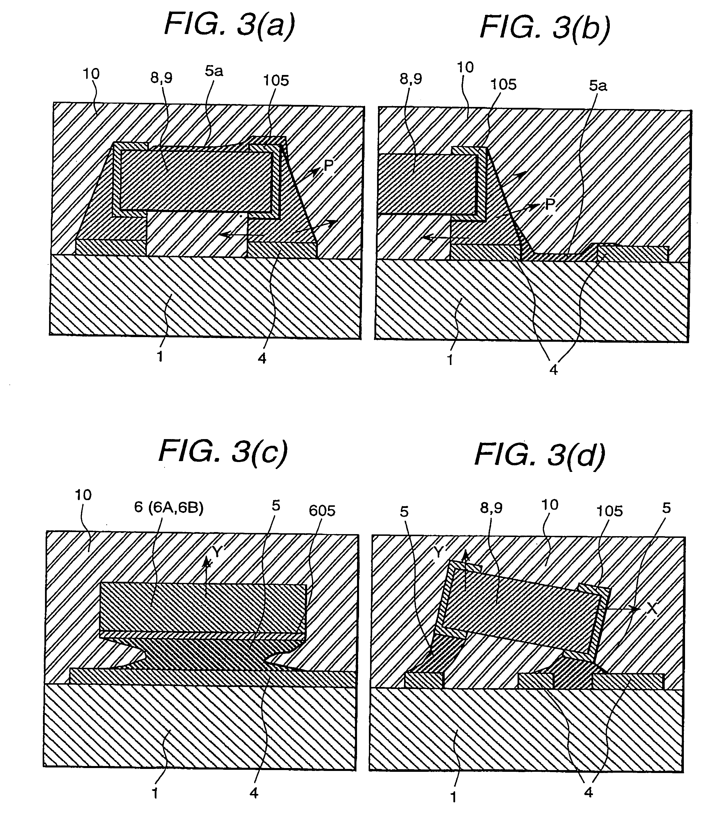
[0058] Semiconductor device 11 is explained in this embodiment.
[0059]FIG. 45 shows a diagrammatic illustration explaining the form of the solders of the present invention.
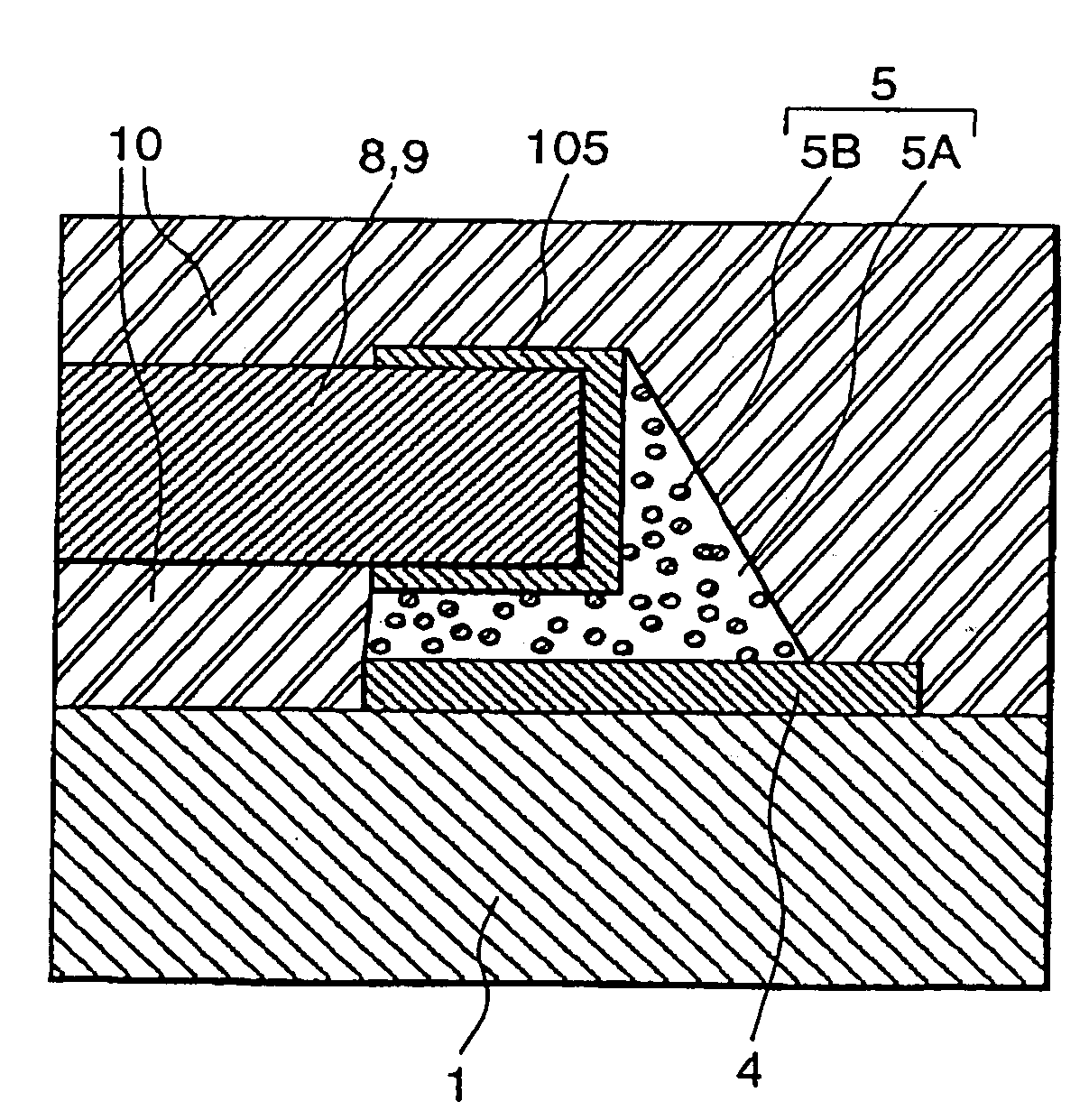
[0060]FIG. 45(a) shows pasty solders 5′ according to a first form. The pasty solders 5′ is the composition made by mixing metal powder (particle size: 15-60. m) 5A for matrix metal comprised of Sn-5 wt % Sb alloy (melting point: 230-240° C.) which becomes the matrix metal after heat-treating of soldering, metal powder (particle size: 15-50 μm and melting point: 779° C.) 5B for dispersion which contains Ag-28 wt % Cu as principal ingredient, and flux material 5C which contains organic substance [weight ratio: WW rosin (100)-adipic acid (1)-tori ethanol amine (1)-aniline hydrochloride (2)]. The amount of addition of the flux material 5C to solders 5′ is about 11 wt %.
[0061] Moreover, the amount of addition is adjusted so that metal powder 5B for dispersion may occupy 50 vol % after heat-treati...
embodiment 2
[0151] (Embodiment 2)
[0152] Semiconductor device 11 obtained by embodiment 1 is applied to structural body 15 according to this embodiment, which is installed on wiring substrate 14, and shown in FIG. 6. Structural body 15 is obtained by bonding electrically external electrode layers 3 of semiconductor device 11 and external wiring 13 comprised of the Cu material of 25. m in thickness, provided on one respect of wiring substrate 14 through external wiring connection layer 12. In this case, Sn-3 wt % Ag-0.5 wtCu solders (melting point: 221° C.) is used as external wiring connection layer 12 (work temperature: 260° C.).
[0153] The coefficient of thermal expansion of matrix material of wiring substrate 14 is different from that of multi-layer ceramics substrate 1 in semiconductor device 1, for example, glass epoxy material (composite material where the epoxy resin is soaked into glass fiber cloth, coeffeicient of thermal expansion: 9.0 ppm / ° C., Young's modulus: 35 GPa). Moreover, the ...
embodiment 3
[0193] (Embodiment 3)
[0194] Structural body 15 obtained by embodiment 2 is applied to the lithium ion accumulator as electronic equipment 100 shown in FIG. 10. Electronic equipment 100 (an accumulator and externals size: 60 mm×30 mm×8 mm) has the following configuration. The accumulator elements such as the positive electrode active material, the negative electrode active material, the positive electrode collector, the negative electrode collector, separators, and the organic electrolyte liquids are housed in metallic case 20 (size: 55 mm×29 mm×7 mm) of having base angle pole type by made of the stainless steel. In this battery, LICoO2 is used as the positive electrode active material and the carbon which has a graphitized structure is used as the negative electrode active material. The positive electrode active material is maintained in the positive electrode collector comprised of Al, and the negative electrode active material is maintained in the negative electrode collector comp...
PUM
| Property | Measurement | Unit |
|---|---|---|
| Particle size | aaaaa | aaaaa |
| Temperature | aaaaa | aaaaa |
| Fraction | aaaaa | aaaaa |
Abstract
Description
Claims
Application Information