Imager photo diode capacitor structure with reduced process variation sensitivity
Active Publication Date: 2005-02-10
APTINA IMAGING CORP
View PDF13 Cites 12 Cited by
Summary
Abstract
Description
Claims
Application Information
AI Technical Summary
This helps you quickly interpret patents by identifying the three key elements:
Problems solved by technology
Method used
Benefits of technology
The present invention addresses the above-described problems and discloses a pixel cell having an array capacitance that i
Problems solved by technology
One problem associated with the FIG. 1 pixel cell 10 is that the floating diffusion region 18 can absorb charge only up to its saturation level.
The surplus charge often leads to image lag and “blooming” in adjacent pixel cells.
Having a high capacitance array capacitor 34 leads to certain problems including image lag and charge transfer inefficiency.
There are, however, several disadvantages associated with reducing the capacitance of array capacitor 34 of pixel cell 10.
Such additional process steps are costly and reduce manufacturing throu
Method used
Image
Click on the blue label to locate the original text in one second.
Reading with bidirectional positioning of images and text.
Examples
Example
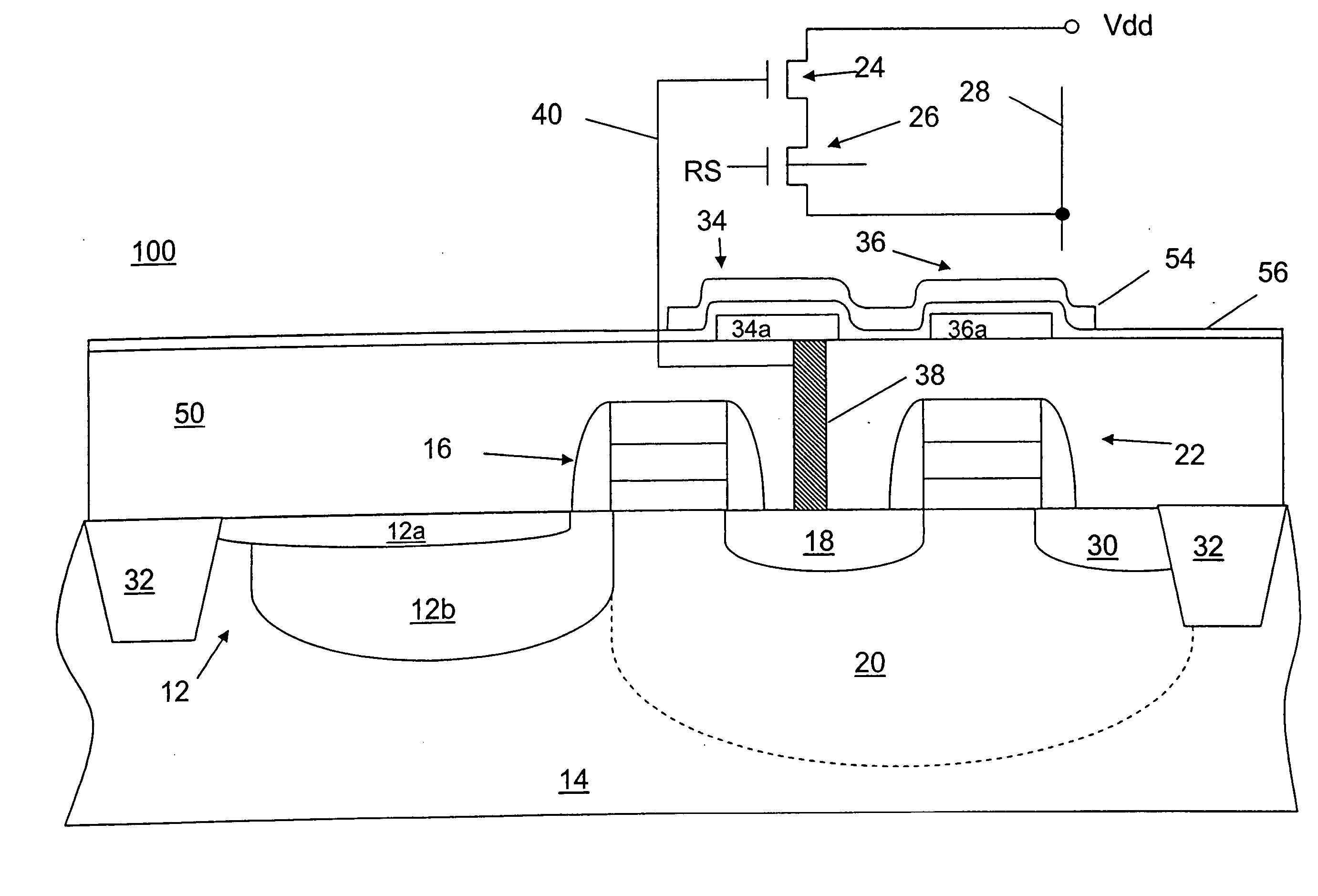
As used herein, the terms “semiconductor substrate” and “substrate” are to be understood to include any semiconductor-based structure. The semiconductor structure should be understood to include silicon, silicon-on-insulator (SOI), silicon-on-sapphire (SOS), silicon-germanium, doped and undoped semiconductors, epitaxial layers of silicon supported by a base semiconductor foundation, and other semiconductor structures. The semiconductor need not be silicon-based. The semiconductor could be germanium or gallium arsenide. When reference is made to the semiconductor substrate in the following description, previous process steps may have been utilized to form regions or junctions in or over the base semiconductor or foundation.
The term “pixel cell,” as used herein, refers to a photo-element unit cell containing a photosensor for converting photons to an electrical signal. For purposes of illustration, a single representative pixel and its manner of formation are illustrated in the fig...
PUM
Abstract
A pixel cell having two capacitors connected in series where each capacitor has a capacitance approximating that of the periphery capacitors and such that the effective capacitance of the series capacitors is smaller than that of each of the periphery capacitors. The series-connected capacitors are coupled to the floating diffusion (FD) region for receiving “surplus” charge from the FD region during saturation conditions.
Description
FIELD OF THE INVENTION The present invention relates generally to an imaging device and more specifically to a complementary metal oxide semiconductor (CMOS) pixel cell having series-connected array capacitors. BACKGROUND OF THE INVENTION Imaging devices, including charge coupled devices (CCD) and complementary metal oxide semiconductor (CMOS) sensors have commonly been used in photo-imaging applications. Exemplary CMOS imaging circuits, processing steps thereof, and detailed descriptions of the functions of various CMOS elements of an imaging circuit are described, for example, in U.S. Pat. No. 6,140,630 to Rhodes, U.S. Pat. No. 6,376,868 to Rhodes, U.S. Pat. No. 6,310,366 to Rhodes et al., U.S. Pat. No. 6,326,652 to Rhodes, U.S. Pat. No. 6,204,524 to Rhodes, U.S. Pat. No. 6,333,205 to Rhodes, and U.S. Patent Appln. Pub. No. 2002 / 0117690. The disclosures of each of the forgoing are hereby incorporated by reference in their entirety. An imager, for example, a CMOS imager include...
Claims
Application Information
Patent Timeline
Application Date:The date an application was filed.
Publication Date:The date a patent or application was officially published.
First Publication Date:The earliest publication date of a patent with the same application number.
Issue Date:Publication date of the patent grant document.
PCT Entry Date:The Entry date of PCT National Phase.
Estimated Expiry Date:The statutory expiry date of a patent right according to the Patent Law, and it is the longest term of protection that the patent right can achieve without the termination of the patent right due to other reasons(Term extension factor has been taken into account ).
Invalid Date:Actual expiry date is based on effective date or publication date of legal transaction data of invalid patent.