Polycrystalline tft uniformity through microstructure mis-alignment

a microstructure and polycrystalline technology, applied in the direction of polycrystalline material growth, crystal growth process, chemically reactive gas, etc., can solve the problems of large device-to-device non-uniformity, increase complexity and thus cost, and difficult to reduce the non-uniformities of semiconductor films and improve the performance characteristics of such films

Inactive Publication Date: 2005-02-17
THE TRUSTEES OF COLUMBIA UNIV IN THE CITY OF NEW YORK
View PDF97 Cites 107 Cited by
  • Summary
  • Abstract
  • Description
  • Claims
  • Application Information

AI Technical Summary

Benefits of technology

[0014] An object of the present invention is to provide a TFT manufacturing technique that provides for control over ...

Problems solved by technology

However, the details of the beam-shaping approach used in conventional ELA methods make it extremely difficult to reduce the non-uniformities in the semiconductor films and to improve the performance characteristics of such films.
For example, in a low-temperature polycrystalline silicon (“LTPS”) process, when the size of the grains becomes comparable to the dimensions of the channel region of the TFT, large device-to-device non-uniformity results.
Such non-uniformity, especially when perpendicular to the current flow, can act as a current barrier.
Unfortunately, the use of lithography requires at lease one extra processing step, which in turn increases complexity and thus costs.
While the s...

Method used


Image

  • Polycrystalline tft uniformity through microstructure mis-alignment
  • Polycrystalline tft uniformity through microstructure mis-alignment
  • Polycrystalline tft uniformity through microstructure mis-alignment

Examples


Embodiment Construction

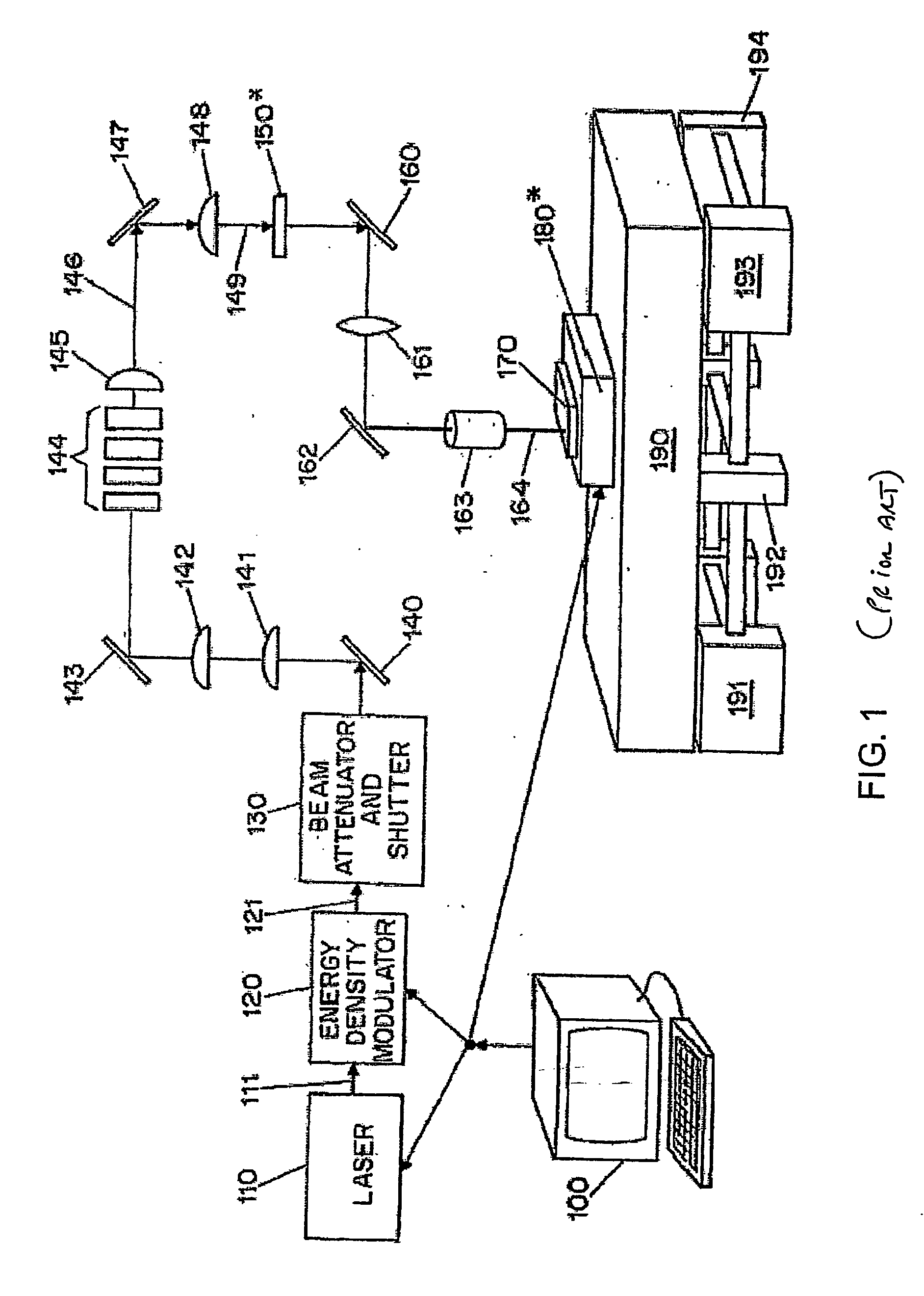
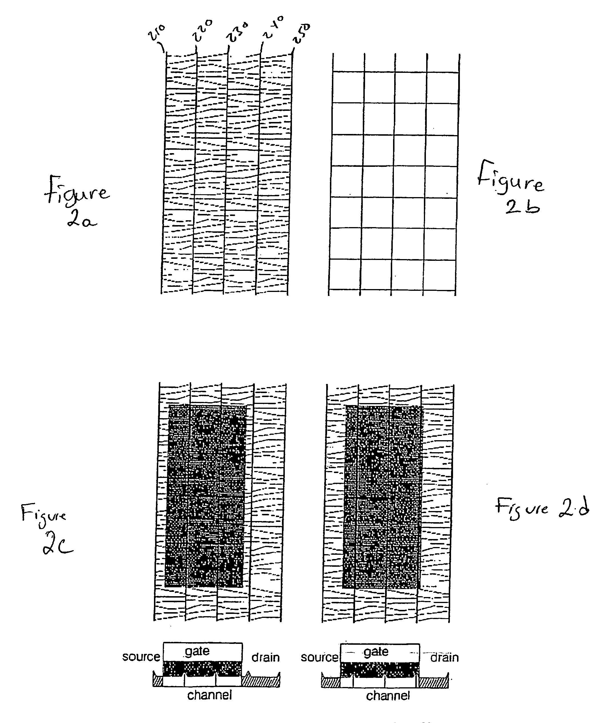
[0027] Referring again to FIGS. 2a-b, exemplary processed silicon thin films using the prior art SLS system of FIG. 1 are shown. In particular, FIG. 2a illustrates a sample processed by irradiating a region with a single excimer laser pulse, micro-translating the sample, and irradiating the region with a second excimer laser pulse. While the following exemplary description of the invention will be with respect to this so-called “2-shot” material as an example, those skilled in the art will appreciate that the present invention is more broadly applicable to silicon thin films that have been processed with n-shot and 2n-shot SLS techniques.

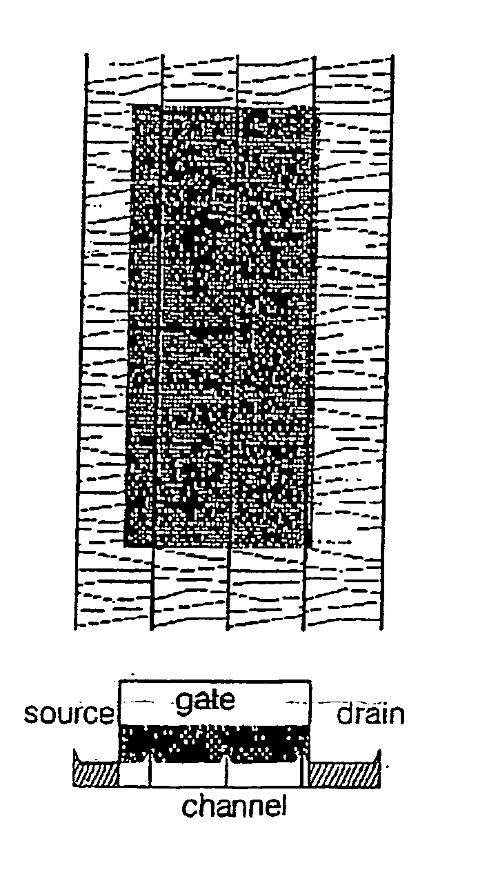
[0028] In accordance with the present invention, active channel regions of TFTs are deliberately tilted relative to the periodic microstructure of the processed thin film. Such tilting may be accomplished by tilting the placement of the channel region itself on the processed thin film, or alternatively, by fabricating a thin film during SLS process...


PUM


Abstract

Methods of making a polycrystalline silicon thin-film transistor having a uniform microstructure. One exemplary method requires receiving a polycrystalline silicon thin film having a grain structure which is periodic in at least a first direction, and placing at least portions (410, 420) of one or more thin-film transistors on the received film such that they are tilted relative to the periodic structure of the thin film.

Description

CROSS-REFERENCE TO RELATED APPLICATIONS [0001] This application is based on U.S. provisional patent application Ser. No. 60 / 315,181, filed Aug. 27, 2001, which is incorporated herein by reference for all purposes and from which priority is claimed.BACKGROUND OF THE INVENTION [0002] 1. Technical Field [0003] The present invention relates to semiconductor processing techniques, and more particularly, techniques for fabricating semiconductors suitable for use at thin-film transistor (“TFT”) devices. [0004] 2. Background Art [0005] Semiconductor films, such as silicon films, are known to be used for providing pixels for liquid crystal display devices and organic light emitting diode display devices. Such films are commonly processed via excimer laser annealing (“ELA”) methods, where an amorphous silicon film is irradiated by an excimer laser to be crystallized. [0006] Significant effort has gone into the refinement of “conventional” ELA (also known as line-beam ELA) processes in the att...

Claims


Application Information

Patent Timeline
IPC IPC(8): C30B13/00C30B13/24C30B29/06H01L21/336H01L21/20H01L29/786
CPCC30B29/06C30B13/24H01L29/04H01L29/78696
Inventor IM, JAMESVAN DER WILT, PAUL CHRISTIAAN
Owner THE TRUSTEES OF COLUMBIA UNIV IN THE CITY OF NEW YORK
Why Eureka
Try Eureka