Plasma processor

Inactive Publication Date: 2005-02-17
TOKYO ELECTRON LTD
View PDF8 Cites 65 Cited by
  • Summary
  • Abstract
  • Description
  • Claims
  • Application Information

AI Technical Summary

Benefits of technology

[0021] As described above, since the matching circuit is scaled down by using a printed circuit board, it is possible to greatly reduce a size of a structure of the propagation system of the microwave. Therefore, the propagation system of the microwave, which includes the microwave generating source, can be mounted on the shield lid as a unit.
[0022] As a result, the maintenance and the repair of the plasma process

Problems solved by technology

Thus, the maintenance and the repairing works of the plasma processing apparatus 2 become quite complex.
Further, as described above, since a length of the rectangular waveguide 32 is relatively long, a multiple reflection of the microwave can easily occur therein and further, a load will be increased accordingl

Method used


Image

  • Plasma processor
  • Plasma processor
  • Plasma processor

Examples


second embodiment

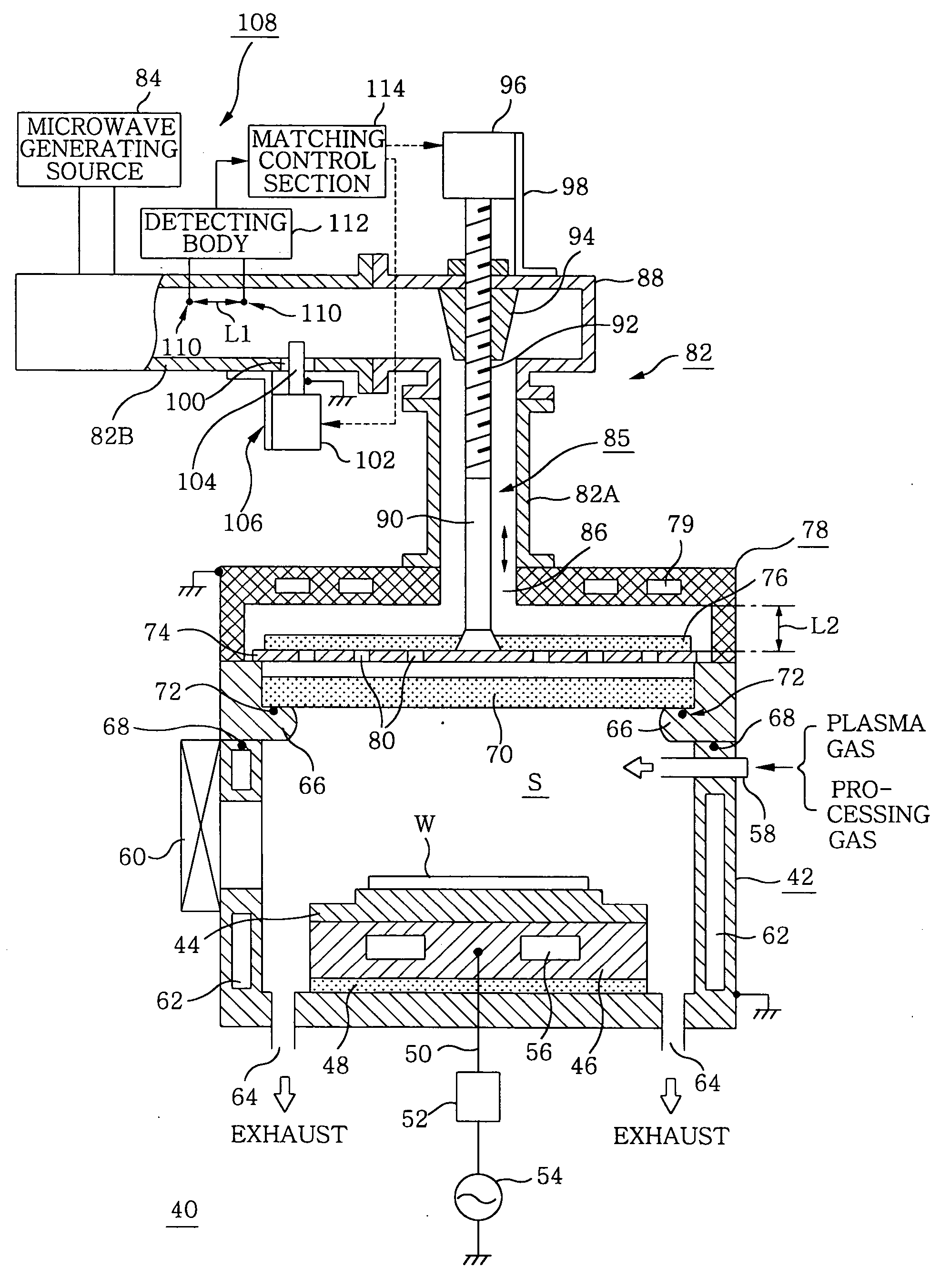
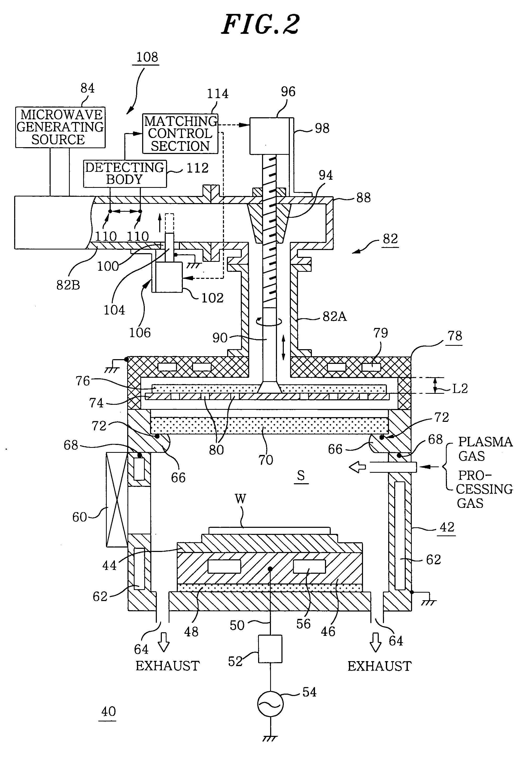
[0066] As illustrated in FIG. 5, in the second preferred embodiment, a planar antenna member 74 is fixed to a supporting frame member 66 provided above a processing vessel 42, and a top end of an internal conductor 90 installed in a coaxial waveguide 82A is fixed to a mode converter 88 by a ridge 94. In addition, a screw driving motor 96 (shown in FIG. 1) is not installed in the Further, a bottom end of the internal conductor 90 is connected to a center of the planar antenna member 74.

[0067] Further, a bottom end of a shield lid 78 is not fixed on a top end of the supporting member 66 but slidably inserted into the top end of the supporting member 66 to thereby make it moveable in a vertical direction. Furthermore, a plurality of, e.g., three, racks 124 (only two racks are shown in FIG. 5) are installed on a side surface of the shield lid 78 along a circumferential direction thereof, the racks 124 being spaced from each other by an approximately identical interval. Each of the rack...

third embodiment

[0071] Only a coaxial waveguide 82A is used as a waveguide 82, as illustrated in FIG. 6. The coaxial waveguide 82A is vertically installed at a central portion of a shield lid 78 and a small-sized matching circuit 130, which is a main characteristic feature of the third embodiment, is installed on an upper end of the coaxial waveguide 82. Further, the matching circuit 130 is connected to a microwave generating source 84 by a coaxial cable 140.

[0072] Specifically, the matching circuit 130 has a base formed by a printed circuit board 132, as illustrated in FIG. 7. A plurality of, e.g., six in FIG. 7, series connections are connected in parallel on the printed circuit board 132, each series connection having a phase advance element, i.e., a capacitor, and a switching device. A phase delay element, i.e., a coil 134, is installed in a middle of the parallel connection described above. The six series connections includes six capacitors C1 to C6 and six switching devices SW1 to SW6 connect...


PUM

PropertyMeasurementUnit
Poweraaaaaaaaaa
Reflectionaaaaaaaaaa

Abstract

A plasma processor with a microwave generating source mounted integrally on a shield lid by miniaturizing a matching circuit. The plasma processor is characterized by comprising a evacuatable processing vessel (42), a workpiece mount base (44) provided in the processing vessel, a microwave transmitting plate (70) provided in the opening section of the top of the processing vessel, a plane antenna member (74) for supplying a microwave into the processing vessel via the microwave transmitting plate, a shield lid (78) so grounded as to cover the top of the plane antenna member, a waveguide (82) for guiding the microwave from a microwave generating source to the plane antenna member, a member elevating mechanism (85) for relatively varying the vertical distance between the plane antenna member and the shield lid, a tuning rod (104) so provided insertably into the waveguide tube, a tuning rod drive mechanism (102) so moving the tuning rod as to adjust its insert amount, and a matching control section (114) for matching adjustment by controlling the elevation amount of the antenna member and the insert amount of the tuning rod.

Description

FIELD OF THE INVENTION [0001] The present invention relates to a plasma processing apparatus for processing a semiconductor wafer and the like by applying thereon a plasma generated by a microwave. BACKGROUND OF THE INVENTION [0002] Along with a recent trend of a high density and a high miniaturization of semiconductor devices, a plasma processing apparatus is used for performing a film forming process, an etching process, an ashing process and the like in a manufacturing process of the semiconductor devices. Especially, since a plasma can be stably generated in an environment at a high vacuum level in which a pressure is comparatively low, e.g., ranging from 0.1 to several tens mTorr, a plasma processing apparatus for processing a wafer by using a high-density plasma generated by a microwave tends to be used. [0003] Such plasma processing apparatus is disclosed in Japanese Patent Laid-Open Publication Nos. 3-191073 and 5-343334 or Japanese Patent Laid-Open Publication No. 9-181052 ...

Claims


Application Information

Patent Timeline
IPC IPC(8): H05H1/46C23C16/511H01J37/32H01L21/205H01P5/103
CPCH01J37/32192H01P5/103H01J37/32568H01J37/32256C23C16/511H01L21/205H01L21/3065H05H1/46
Inventor KASAI, SHIGERUYAMAMOTO, NOBUHIKOADACHI, HIKARUOSADA, YUKI
Owner TOKYO ELECTRON LTD
Why Eureka
Try Eureka