Solid state image sensing device having pixels provided with barrier layer underneath transistor regions and camera using said device
- Summary
- Abstract
- Description
- Claims
- Application Information
AI Technical Summary
Benefits of technology
Problems solved by technology
Method used
Image

Examples
first embodiment
[0053] First Embodiment
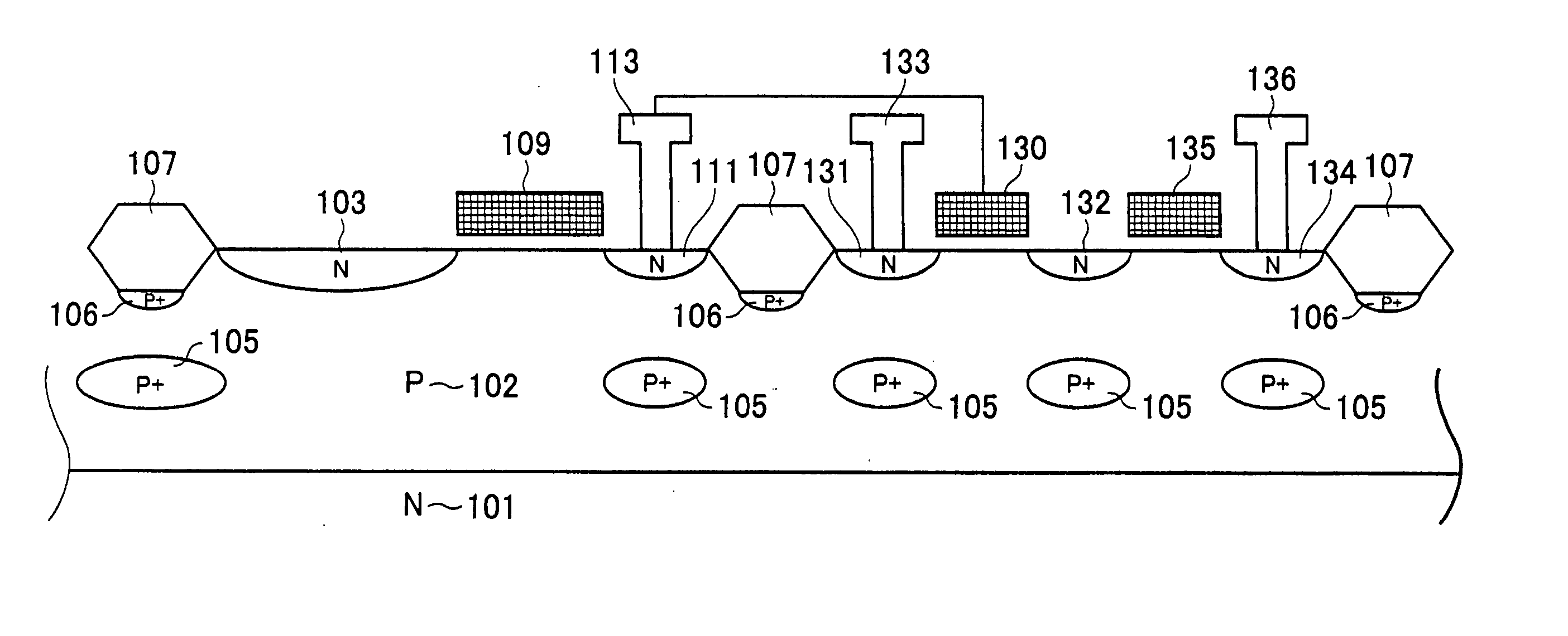
[0054]FIG. 1 is a schematic sectional view of a solid-state image sensing device according to a first embodiment of the present invention.
[0055] In FIG. 1, reference numeral 101 represents a semiconductor substrate having a first-conductivity-type (n-type in this case by way of example), 102 is a p well which is a second-conductivity-type semiconductor region, and 103 is an n-type semiconductor region which is formed in the p well 102 and which is a first-conductivity-type semiconductor region. The p well 102 and the n-type semiconductor region 103 constitute a photodiode. Signal charge that is generated from incident light is stored in the n-type semiconductor region 103. Reference numeral 111 represents a drain region of a transfer transistor, which is a first transistor, for transferring signal charge generated by the photodiode. The drain region has the first conductivity type and serves as an FD region and an n-type semiconductor region formed in the p w...
second embodiment
[0065] Second Embodiment
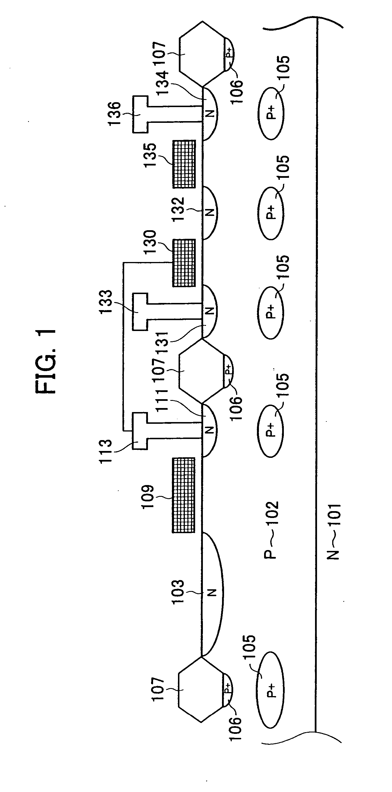
[0066]FIG. 2 is a schematic sectional view of a solid-state image sensing device according to a second embodiment of the present invention.
[0067] More specifically, FIG. 2 is a schematic sectional view of a solid-state image sensing device having a photodiode, a transfer transistor and a reset transistor for resetting an FD electrode 211. Thus, this solid-state image sensing device has a reset transistor, serving as a second transistor, for resetting the FD electrode 211.
[0068] In FIG. 2, reference numeral 223 represents a gate electrode of the reset transistor for resetting the FD electrode 211 and reference numeral 224 represents a drain region of the reset transistor and is connected to a power-supply line 226.
[0069] This embodiment is different from the first embodiment described above in that a potential barrier 205 is also provided under the gate electrode 223 of the second transistor. Thus, the potential barrier 205 reduces the amount of signal char...
third embodiment
[0077] Third Embodiment
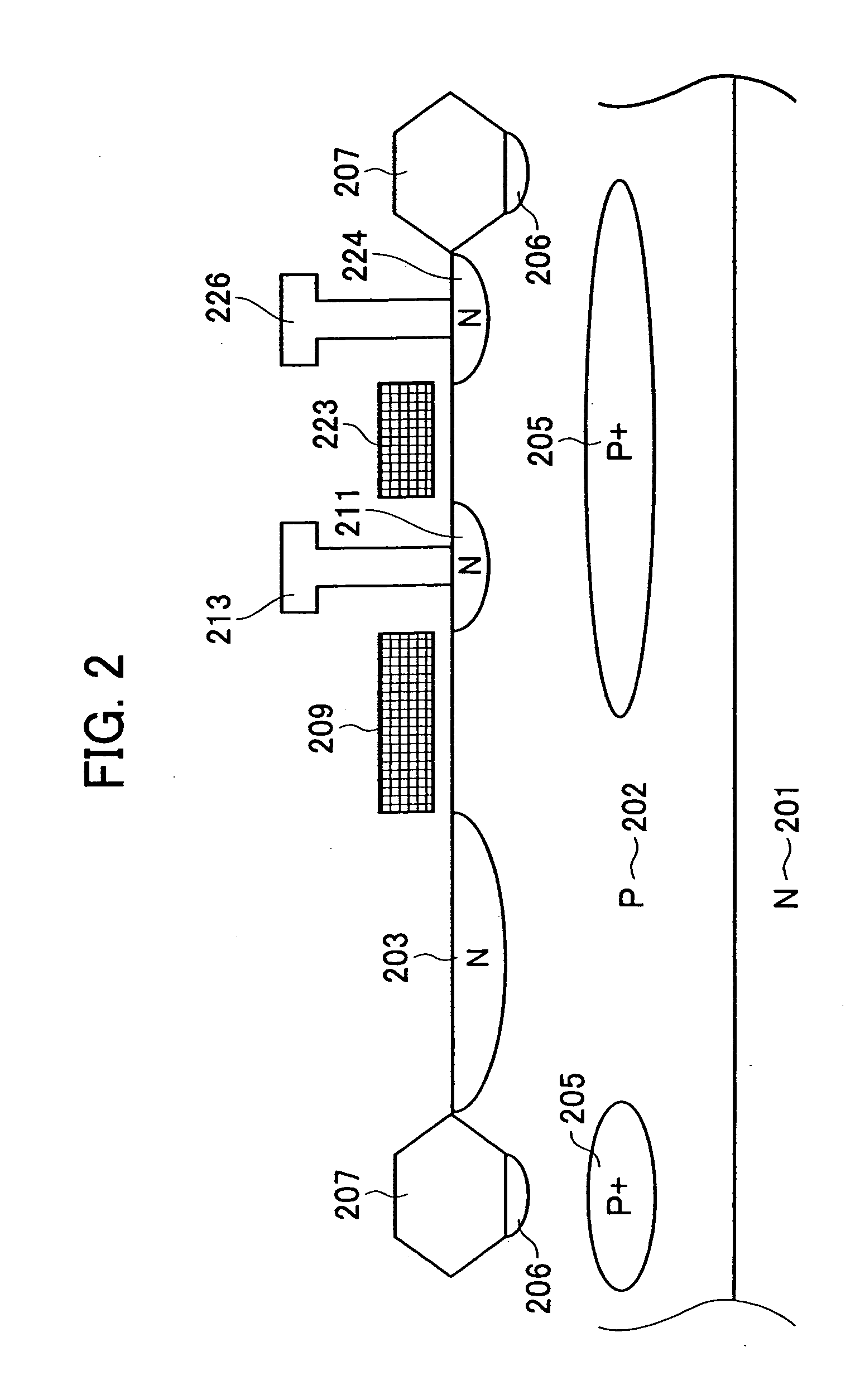
[0078]FIG. 3 is a schematic sectional view of a solid-state image sensing device according to a third embodiment of the present invention.
[0079] Specifically, FIG. 3 is a schematic sectional view of a solid-state image sensing device having a photodiode, a transfer transistor, and a reset transistor for resetting an FD electrode 311.
[0080] Referring to FIG. 3, an n well or n-type semiconductor region 303 is provided as a first-conductivity-type semiconductor region at a layer above an n-type semiconductor substrate 301. A p-type semiconductor region 302 is provided as a second-conductivity-type semiconductor region. The p-type semiconductor region 302 and the n-type semiconductor region 303 constitute a photodiode. A first-conductivity-type signal-charge storing region 312 collects and stores signal charge generated by the photodiode and has a doping concentration higher than the n-type semiconductor region 303.
[0081] The difference between the configuratio...
PUM
 Abstract
Description
Claims
Application Information